Tunneling Effect
In a normally-doped P-N junction, the depletion layer is relatively wide and a potential barrier exists across the junction. The charge carriers on either side of the junction cannot cross over unless they possess sufficient energy to overcome this barrier (0.3 V for Ge and 0.7 V for Si).
As is well-known, width of the depletion region depends directly on the doping density of the semiconductor. If a P-N junction is doped very heavily (1000 times or more), its depletion layer becomes extremely thin (about 0.00001 mm).
It is found that under such conditions, many carriers can ‘punch through’ the junction with the speed of light even when they do not possess enough energy to overcome the potential barrier. Consequently, large forward current is produced even when the applied bias is much less than 0.3 V.
This conduction mechanism in which charge carriers (possessing very little energy) bore through a barrier directly instead of climbing over it is called tunneling.
Explanation of Tunneling Effect
Energy band diagrams (EBD) of N-type and P-type semiconductor materials can be used to explain this tunneling phenomenon. Fig. 1 shows the energy band diagram of the two types of silicon separately.
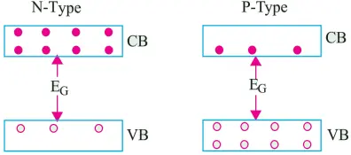
As explained earlier, in the N-type semiconductor, there is increased concentration of electrons in the conduction band. It would be further increased under heavy doping. Similarly, in a P-type material, there is increased concentration of holes in the valence band for similar reasons.
(a) No Forward Bias: When the N-type and P-type materials are joined, the EBD under no-bias condition becomes as shown in Fig. 2(a). The junction barrier produces only a rough alignment of the two materials and their respective valence and conduction bands.
As seen, the depletion region between the two is extremely narrow due to very heavy doping on both sides of the junction. The potential hill is also increased as shown.
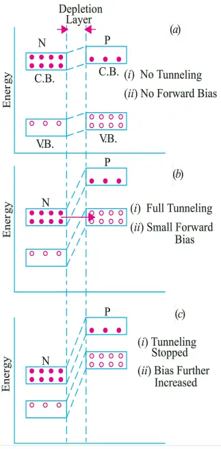
(b) Small Forward Bias: When a very small forward voltage (≅ 0.1 V) is applied, the EBDs become as shown in Fig. 2(b). Due to the downward movement of the N-region, the P-region valence band becomes exactly aligned with the N-region conduction band.
At this stage, electrons tunnel through the thin depletion layer with the velocity of light thereby giving rise to a large current called peak current Ip.
(c) Large Forward: Bias When the forward bias is increased further, the two bands get out of alignment as shown in Fig. 2(c). Hence, tunneling of electrons stops thereby decreasing the current.
Since current decreases with increase in applied voltage (i.e. dV/dI is negative), the junction is said to possess negative resistance at this stage. This resistance increases throughout the negative region. However, it is found that when applied forward voltage is increased still further, the current starts increasing once again as in a normal junction diode.
Construction of Tunnel Diode
It is a high-conductivity two-terminal P-N junction diode having doping density about 1000 times higher as compared to an ordinary junction diode. This heavy doping produces following three unusual effects:
- Firstly, it reduces the width of the depletion layer to an extremely small value (about 0.00001 mm).
- Secondly, it reduces the reverse breakdown voltage to a very small value (approaching zero) with the result that the diode appears to be broken down for any reverse voltage.
- Thirdly, it produces a negative resistance section on the V/I characteristic of the diode.
It is called a tunnel diode because due to its extremely thin depletion layer, electrons are able to tunnel through the potential barrier at relatively low forward bias voltage (less than 0.05 V).
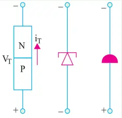
Such diodes are usually fabricated from germanium, gallium-arsenide (GaAs) and gallium antimonide (GaSb). The commonly-used schematic symbols for the diode are shown in Fig. 3. It should be handled with caution because being a low-power device, it can be easily damaged by heat and static electricity.
V-I Characteristic of Tunnel Diode
It is shown in Fig. 4. As seen, forward bias produces immediate conduction i.e. as soon as forward bias is applied, significant current is produced. The current quickly rises to its peak value Ip when the applied forward voltage reaches a value Vp (point A).
When forward voltage is increased further, diode current starts decreasing till it achieves its minimum value called valley current Iv corresponding to valley voltage Vv (point B). For voltages greater than Vv, current starts increasing again as in any ordinary junction diode.
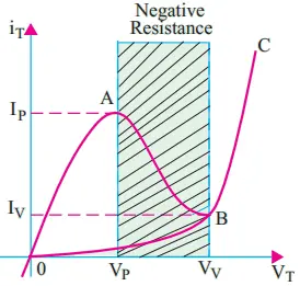
As seen from Fig. 4, between the peak point A and valley point B, current decreases with increase in the applied voltage. In other words, tunnel diode possesses negative resistance (— RN) in this region. In fact, this constitutes the most useful property of the diode.
Instead of absorbing power, a negative resistance produces power. By offsetting losses in L and C components of a tank circuit, such a negative resistance permits oscillations. Hence, a tunnel diode is used as a very high frequency oscillator.
Another point worth noting is that this resistance increases as we go from point A to B because as voltage is increased, current keeps decreasing which means that diode negative resistance keeps increasing.
Tunneling Theory
At zero forward bias, the energy levels of conduction electrons in N-region of the junction are slightly out of alignment with the energy levels of holes in the P-region.
As the forward voltage is slightly increased, electron levels start getting aligned with the hole levels on the other side of junction thus permitting some electrons to cross over. This kind of junction crossing is called tunneling.
As voltage is increased to peak voltage (VP), all conduction band electrons in the N-region are able to cross over to the valence band in the P-region because the two bands are exactly aligned. Hence, maximum current (called peak current IP) flows in the circuit.
After VP, as the applied voltage is increased, current starts decreasing because the two bands start gradually getting out of alignment. It reaches minimum value (called valley current) when the two are totally out of alignment at a forward bias of VV (valley voltage).
For voltages greater than VV, current starts increasing again exactly as it does in the case of an ordinary P-N junction diode.
Tunneling is much faster than normal crossing which enables a tunnel diode to switch ON and OFF much faster than an ordinary diode. That is why a tunnel diode is extensively used in special applications requiring very fast switching speeds like high-speed computer memories and high frequency oscillators etc.
Diode Parameters
(i) Negative Resistance (– RN): It is the resistance offered by the diode within the negative-resistance section of its characteristic (shown shaded in Fig. 4). It equals the reciprocal of the slope of the characteristic in this region.
It may also be found from the following relation RN = − dV/dI.
Its value depends on the semiconductor material used (varying from − 10 Ω to − 200 Ω).
(ii) IP/ IV Ratio: It is almost as important factor (particularly for computer applications) as the negative resistance of the diode.
Silicon diodes have a low IP/IV ratio of 3:1 and their negative resistance can be approximated from RN = − 200/IP. Such diodes are used mainly for switches operating in high ambient temperatures.
Germanium diodes have an IP/IV ratio of 6:1 and negative resistance formula RN = − 120/IP. GaAs diodes (used exclusively in oscillators) have an IP/IV ratio of about 10:1 and a negative resistance nearly equal to that of silicon diodes.
The minimum IP/IV ratio for GaSb diode is about 12:1 and has the lowest resistance of all given by RN = − 60/IP. Hence, such diodes have the lowest noise.
Equivalent Circuit
The equivalent circuit of a tunnel diode is shown in Fig. 5.
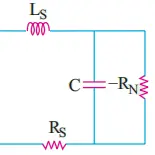
- The capacitance C is the junction diffusion capacitance (1 to 10 pF) and (− RN) is the negative resistance.
- The inductor LS is due mainly to the terminal leads (0.1 to 4 nH).
- The resistance RS is due to the leads, ohmic contact and semiconductor materials (1 − 5 Ω).
These factors limit the frequency at which the diode may be used. They are also important in determining the switching-speed limit.
Biasing the Tunnel Diode
The tunnel diode has to be biased from some dc source for fixing its Q-point on its characteristic when used as an amplifier or as an oscillator and modulator.
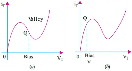
The diode is usually biased in the negative region [Fig. 6(a)]. In mixer and relaxation oscillator applications, it is biased in the positive-resistance region nearest zero [Fig. 6(b)].
Applications of Tunnel Diode
Tunnel diode is commonly used for the following purposes:-
1. as an ultrahigh-speed switch – due to tunneling mechanism which essentially takes place at the speed of light. It has a switching time of the order of nanoseconds or even picoseconds.
2. as logic memory storage device − due to triple-valued feature of its curve for current.
3. as microwave oscillator at a frequency of about 10 GHz − due to its extremely small capacitance and inductance and negative resistance.
4. in relaxation oscillator circuits − due to its negative resistance. In this respect, it is very similar to the unijunction transistor.
Advantages and Disadvantages of Tunnel Diode
The advantages of a tunnel diode are:
- low noise,
- ease of operation,
- high speed,
- low power,
- insensitivity to nuclear radiations
The disadvantages are:
- the voltage range over which it can be operated properly is 1 V or less;
- being a two-terminal device, it provides no isolation between the input and output circuits.
Tunnel Diode Oscillator
The basic job of an oscillator is to convert dc power into ac power. Ordinarily, we do not expect an ac signal from a circuit which has no input ac source. But the circuit shown in Fig. 7 does exactly that as explained below.
The value of R is so selected as to bias the diode D in the negative-resistance region A − B. The working or quiescent point Q is almost at the centre of the curve A − B.
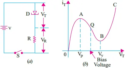
When S is closed, the current immediately rises to a value determined by R and the diode resistance which are in series. The applied voltage V divides across D and R according to the ratio of their resistances.
However, as VT exceeds VP, diode is driven into the negative area and its resistance starts to increase. Hence, VT increases further till it becomes equal to valley voltage VV (point B). At this point, further increase in VT drives the diode into the positive resistance region BC [Fig. 7(b)].
The resulting increase in current now increases VR but correspondingly decreases VT, thereby bringing the diode back into the negative-resistance region.
This decrease in VT increases the circuit current till point A is reached when VT equals VP. It describes one cycle of operation.
In this way, the circuit will continue to oscillate back and forth through the negative-resistance region i.e. between points A and B on its characteristic. Its output across R is like a sine wave.
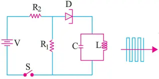
Fig. 8 shows a practical circuit. Here, R2 sets the proper bias level for the diode whereas R1 (in parallel with the LC tank circuit) sets proper current level for it. The capacitor CC is the coupling capacitor. As the switch S is closed, the diode is set into oscillations whose frequency equals the resonant frequency of the tank.