Photodiode
It is a two-terminal junction device which is operated by first reverse-biasing the junction and then illuminating it. A reverse-biased P-N junction has a small amount of reverse saturation current Is (or I0) due to thermally-generated electron-hole pairs. In silicon, Is is the range of nano-amperes.
The number of these minority carriers depends on the intensity of light incident on the junction. When the diode is in glass package, light can reach the junction and thus change the reverse current. The basic biasing arrangement, construction and symbols of a photodiode are shown in Fig. 1.
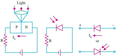
As seen, a lens has been used in the cap of the unit to focus maximum light on the reverse-biased junction. The active diameter of these devices is about 2.5 mm but they are mounted in standard TO-5 packages with a window to allow maximum incident light.
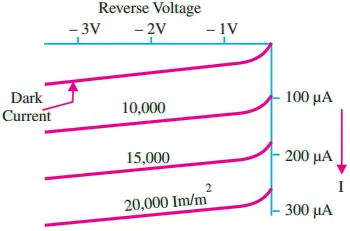
The characteristics of Fig. 2 show that for a given reverse voltage, Iλ (or Is) increases with increase in the level of illumination. The dark current refers to the current that flows when no light is incident. By changing the illumination level, reverse current can be changed. In this way, reverse resistance of the diode can be changed by a factor of nearly 20.
A photodiode can turn its current ON and OFF in nanoseconds. Hence, it is one of the fastest photo-detectors. It is used where it is required to switch light ON and OFF at a maximum rate. Applications of a photodiode include:-
- detection, both visible and invisible;
- demodulation;
- switching;
- logic circuit that require stability and high speed;
- character recognition;
- optical communication equipment;
- encoders etc.
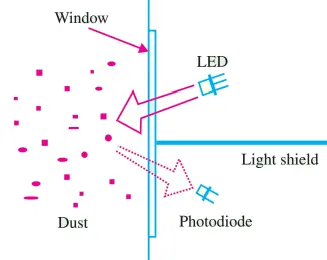
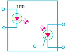
Dust Sensor: Fig. 3 shows a combination of an LED and a photodiode used as a dust sensor. As seen, the light emitted from the LED gets reflected by the dust particles. The reflected light is collected by the photodiode and is converted into an electrical signal. The dust sensor is employed in cleaners. The combination of an LED and a photodiode is also used as:
- a paper sensor in facsimile machines,
- as a tape-end sensor in videotape recorders/players, and
- as a dirt detector for rinsing in washing machines.
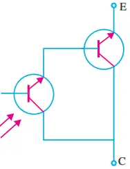
Phototransistor
It is light-sensitive transistor and is similar to an ordinary bipolar junction transistor (BJT) except that it has no connection to the base terminal. Its operation is based on the photodiode that exists at the CB junction.
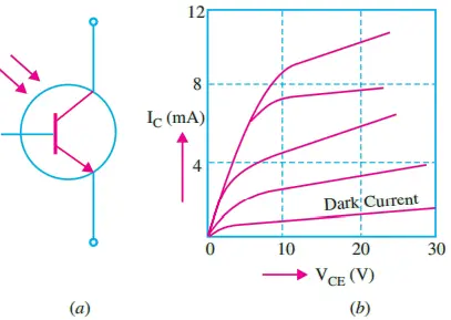
Instead of the base current, the input to the transistor is provided in the form of light as shown in the schematic symbol of Fig. 4(a).
Silicon NPNs are mostly used as photo transistors. The device is usually packed in a TO-type can with a lens on top although it is sometimes encapsulated in clear plastic.
When there is no incident light on the CB junction, there is a small thermally-generated collector-to-emitter leakage current ICEO which, in this case, is called dark current and is in the nA range.
When light is incident on the CB junction, a base current Iλ is produced which is directly proportional to the light intensity. Hence, collector current IC = β Iλ Typical collector characteristic curves of a phototransistor are shown in Fig. 4(b). Each individual curve corresponds to a certain value of light intensity expressed in mW/cm2.
As seen, IC increases with light intensity. The phototransistor has applications similar to those of a photodiode. Their main differences are in the current and response time. The photo-transistor has the advantages of greater sensitivity and current capacity than photodiodes. However, photodiodes are faster of the two, switching in less than a nanosecond.
Photodarlington
As shown in Fig. 5 a photodarlington consists of a phototransistor in a Darlington arrangement with a common transistor. It has a much greater sensitivity to incident radiant energy than a phototransistor because of higher current gain. However, its switching time of 50 µs is much longer than the phototransistor (2 µs) or the photodiode (1 ns). Its circuit symbol is shown in Fig. 5.
Applications: Photodarlingtons are used in a variety of applications some of which are given below.
A light-operated relay is shown in Fig. 6. The phototransistor T1 drives the bipolar transistor T2. When sufficient light falls on T2, it is driven into saturation so that IC is increased manifold. This collector current while passing through the relay coil energizes the relay.
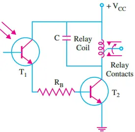
Fig. 7 shows a dark-operated relay circuit i.e. one in which relay is de-energized when light falls on the phototransistor. Here, T1 and R form a potential divider across VCC. With insufficient light incident on T1, transistor T2 is biased ON thereby keeping the relay energized.
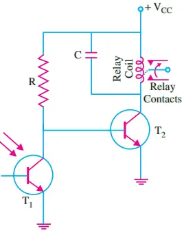
However, when there is sufficient light, T1 turns ON and pulls the base of T2 low thereby turning T2 OFF and hence, de-energizing the relay.
Such relays are used in many applications such as (i) automatic door activators, (ii) process counters and (iii) various alarm systems for smoke or intrusion detection.
Light-activated SCR (LASCR)
The operation of a LASCR is essentially similar to that of a conventional SCR except that it is light-triggered (Fig. 8). Moreover, it has a window and lens which focuses light on the gate junction area. The LASCR operates like a latch.
- It can be triggered ON by a light input on the gate area but does not turn OFF when light source is removed.
- It can be turned OFF only by reducing the current through it below its holding current.
- Depending on its size, a LASCR is capable of handling larger amount of current that can be handled by a photodiode or a photo-transistor.
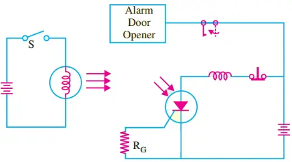
Fig. 8 shows how a LASCR can be used for energizing a latching relay. The input dc source turns on the electric lamp and the resulting incident light triggers the LASCR into conduction. The anode current energizes the relay and closes the contact. It is seen that the input dc source is electrically isolated from the rest of the circuit.
Optical Isolators
Optical isolators are designed to electrically isolate one circuit from another while allowing one circuit to control the other. The usual purpose of isolation is to provide protection from high-voltage transients, surge voltages and low-level electrical noise that could possibly result in an erroneous output or damage to the device. Such isolators allow interfacing of circuits with different voltage levels and different grounds etc.
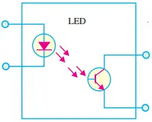
An optical isolator (or coupler) consists of a light source such as LED and a photo-detector such as a photo transistor as shown in Fig. 9 and is available in a standard IC package.
When LED is forward-biased, the light produced by it is transferred to the phototransistor which is turned ON thereby producing current through the external load.
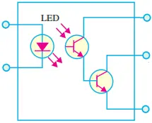
Fig. 10 shows a Darlington transistor coupler which is used when increased output current capability is needed beyond that provided by the phototransistor output.
The LASCR output coupler of Fig. 11 can be used in applications where a low-level input voltage is required to latch a high voltage relay for activating some kind of electro-mechanical device.