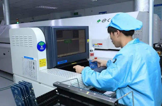
In SMT (Surface Mount Technology) production, inspection is a critical part of the entire process. From solder paste printing to component placement and reflow soldering, even a small mistake can cause PCB failure, rework, or in some cases, entire batches to be scrapped. Among the many inspection methods available, AOI (Automated Optical Inspection) has become the most widely used and indispensable solution in SMT manufacturing because of its speed, accuracy, and consistency.
Many people ask the same question: SMT inspection can be done in several ways, including manual visual inspection, ICT (In-Circuit Testing), and X-ray inspection, so why has AOI become the preferred choice? The answer is straightforward. AOI aligns extremely well with the core demands of SMT manufacturing: high density, high speed, and high consistency. It addresses the limitations that other inspection methods cannot balance as effectively. In this article, we will look at the core pain points of SMT production and explain why AOI has become the mainstream inspection solution.
The Inspection Challenges in SMT Explain Why Manual Inspection Has Been Phased Out
Components Have Become Too Small for Reliable Manual Inspection: Today’s SMT lines commonly use components in 0402 and 0201 packages, and even ultra-small packages such as 01005 and 008004 are now seen in advanced applications. The lead pitch on these components can be less than 0.1 mm, and the solder joints are smaller than the tip of a needle. Even with magnification, it is extremely difficult for the human eye to reliably identify subtle defects such as insufficient solder, weak solder joints, or slight lead misalignment.
What makes the problem even more serious is that a high-end PCB may contain thousands of densely packed components. Every solder joint, polarity mark, and placement position must be checked. Human eyesight and concentration simply cannot keep up with that level of precision, which leads to high rates of missed defects and incorrect judgments.
Production Is Too Fast for Manual Inspection to Keep Up: Modern SMT placement machines can place tens of thousands, or even more than one hundred thousand, components per hour. A complex PCB can move through placement and soldering in just a few minutes. By comparison, a manual inspection of the same board may take at least five to ten minutes, and often longer. That pace does not match the rhythm of the production line and can quickly create bottlenecks that reduce overall efficiency.
There is also a practical human factor. Manual inspection requires sustained concentration, and fatigue increases quickly over long shifts. As fatigue builds, the rate of missed defects rises sharply. According to industry data, the miss rate in manual inspection is often above 10% to 15%, while SMT assembly services may require defect levels below 0.1%. Manual inspection simply cannot meet that standard.
Quality Requirements Are Higher Than Ever, and Manual Inspection Cannot Deliver Consistency: Industries such as consumer electronics, automotive electronics, and medical devices demand a very high level of quality consistency. Boards of the same model within the same production batch must be inspected against the same standard every time. Results cannot vary based on the inspector’s experience, mood, or level of fatigue.
Manual inspection is highly subjective. A new operator and an experienced operator may judge the same board differently, and even the same person may make different decisions at different times of day. This lack of consistency increases the risk that defective boards will move to the next process, or even reach the customer, leading to product failures, complaints, rework costs, and brand damage.
These three pain points are exactly why manual inspection has gradually been phased out, and why AOI has become a practical necessity in SMT production process.
AOI’s Core Advantages Match the Three Main Requirements of SMT
High-Precision Inspection That Supports High-Density SMT Production: AOI uses high-resolution cameras, multi-angle lighting, and image analysis algorithms to perform extremely detailed inspection. In many cases, it can identify defects at the 0.01 mm level. Whether the issue is component offset on a 01005 package, weak soldering on leads, insufficient paste, solder bridging, or even small foreign matter on the PCB surface, AOI can detect it with a high level of accuracy.
Just as important, AOI can adapt to different inspection points in SMT production. It can be used for bare board inspection, solder paste-related inspection, and post-reflow inspection. That means it can cover a wide range of defect types across the SMT process without requiring completely different inspection platforms for each stage.
Compared with other methods, ICT mainly checks electrical continuity and cannot identify visible appearance defects. X-ray inspection is mainly used for hidden solder joints such as those under BGA packages, but it cannot cover full surface-level visual inspection and is more expensive. AOI fills the gap by offering high-precision, full-surface inspection that fits the trend toward dense layouts and fine-pitch assembly.
High-Speed Inspection That Matches SMT Line Throughput: AOI inspection speed is well aligned with SMT production pace. A complex PCB can often be inspected in just 3 to 10 seconds, which is dramatically faster than manual inspection. AOI can also be integrated directly into the line, allowing boards to move from placement or reflow straight into inspection without interrupting workflow.
AOI can run continuously without the fatigue issues that affect human inspectors. There are no breaks, no shift-related attention drops, and no slowdown caused by manual review at every board. Industry experience shows that after AOI is implemented, SMT inspection efficiency can improve by more than 80%, while overall line productivity may increase by 30% to 50%.
High Consistency Through Standardized Inspection Logic: AOI operates using predefined standards. A known-good PCB image is typically loaded as a golden reference, and each board is compared against that standard at the pixel level. The system then automatically determines whether the board passes or fails based on inspection rules, without subjective judgment.
This standardized process removes the variation that comes with manual inspection. In many applications, the missed defect rate can be kept below 0.5%, while defect detection rates can exceed 99%. For industries such as automotive electronics and medical devices, where reliability standards are extremely strict, this consistency is one of the biggest reasons AOI is so valuable.
Lower Total Cost and Better Traceability: Over time, AOI can significantly reduce total manufacturing cost. On one hand, it reduces labor requirements, since one AOI machine may replace the work of five to eight inspectors. On the other hand, it catches defects earlier, before defective boards move deeper into the process. That lowers rework costs, scrap costs, and downstream quality losses. Industry estimates show that the earlier a defect is found in SMT production, the lower the repair cost. When AOI identifies issues immediately after solder paste printing or component placement, rework cost can be reduced by more than 60%.
AOI also creates traceable inspection data. It can automatically record defect type, defect location, inspection time, and batch information for each PCB. These records can be uploaded to MES systems and used to analyze root causes, such as solder paste offset, unstable oven temperature, or placement accuracy issues. That allows manufacturers to improve the process and reduce defect rates at the source.
AOI’s Core Application Scenarios in SMT
Inspection After Solder Paste Printing: This is a front-end inspection stage. The focus is on solder paste print quality, including offset, insufficient paste, excessive paste, peaked deposits, bridging, and pad contamination. If a problem is found at this stage, printer parameters can be adjusted immediately. That prevents larger numbers of defects later during placement and soldering, making this a very cost-effective form of defect prevention.
Inspection After Component Placement: At this stage, AOI checks placement quality, including missing components, wrong components, offset placement, reversed polarity, tombstoning, and lifted leads. It helps identify placement machine deviations before the board enters reflow, which reduces the difficulty and cost of downstream repair.
Inspection After Reflow Soldering: This is the most common and most important AOI application in SMT. The system inspects all visible post-soldering defects, including weak solder joints, cold solder joints, bridging, insufficient solder, excessive solder, solder balls, component shift, and lifted parts. This stage is critical because it screens out defective boards before they move to later steps such as through-hole insertion, final assembly, or shipment.
For advanced SMT lines, such as those used in AI servers or automotive electronics, 3D AOI is often added as well. By measuring height information, 3D AOI can more accurately detect solder volume, component lift, and certain edge solder joint conditions that are harder for 2D AOI to identify.
Why AOI Remains Irreplaceable Compared With Other Inspection Methods:Many people ask: if inspection methods such as ICT and X-ray already exist, why is AOI still necessary? The answer is that each inspection method serves a different purpose. AOI stands out because it combines full-process visual coverage, high accuracy, and high inspection speed in a way that other methods cannot fully replace.
| Inspection Method | Key Strengths | Main Limitations | Best-Fit Application |
| AOI (Automated Optical Inspection) | Full visual inspection, high accuracy, high speed, moderate cost, traceability | Cannot detect internal defects or hidden solder joints | Full-process visual inspection in SMT production (mainstream application) |
| Manual Visual Inspection | Low initial cost, flexible | Low efficiency, high miss rate, inconsistent standards | Small-volume, low-precision PCB inspection (now largely phased out) |
| ICT (In-Circuit Testing) | Detects electrical continuity, internal opens, and shorts | Cannot detect visual defects, requires custom test fixtures | Electrical performance testing for PCBs (supplementary application) |
| X-Ray Inspection | Detects hidden solder joints such as BGA and QFN | High cost, slower speed, cannot cover all visible defects | Hidden solder joint inspection for high-end PCBs (supplementary application) |
Conclusion
As SMT manufacturing continues to move toward higher density, faster throughput, and greater reliability, AOI has evolved from an optional inspection tool into a standard part of the SMT production line. Without AOI, it becomes much harder to support large-scale production of high-density PCBs, maintain consistent product quality, or control overall manufacturing cost.
The real value of AOI is not only in defect detection. It also helps prevent defects earlier, supports process improvement, and enables manufacturers to improve quality, increase efficiency, and reduce cost at the same time. Whether in consumer electronics, telecom equipment, automotive electronics, or AI servers, AOI plays a quiet but essential role behind every high-quality PCB.
For that reason, when choosing the right EMS PCB Manufacturer, one important point to check is whether the SMT line is equipped with AOI systems.