How do solar pv panels generate electricity ?
Photovoltaic (PV) conversion is the direct conversion of sunlight into electricity with no intervening heat engine. PV devices are solid state; therefore, they are rugged and simple in design and require very little maintenance. Perhaps the biggest advantage of solar PV devices is that they can be constructed as stand-alone systems to give outputs from microwatts to megawatts.
That is why they have been used as the power sources for calculators, watches, water pumping, remote buildings, communications, satellites and space vehicles, and even megawatt-scale power plants.
PV panels can be made to form components of a building skin, such as roof shingles and wall panels. With such a vast array of applications, the demand for photovoltaics is increasing every year.
Semiconductors
A basic understanding of the atomic structure is quite helpful in understanding the behavior of semiconductors and their use as PV energy conversion devices.
For any atom, the electrons arrange themselves in orbitals around the nucleus so as to result in the minimum amount of energy.
In elements that have electrons in multiple shells, the innermost electrons have minimum energy and, therefore, require the maximum amount of externally imparted energy to overcome the attraction of the nucleus and become free.
Electrons in the outermost band of subshells are the only ones that participate in the interaction of an atom with its neighboring atoms. If these electrons are very loosely attached to the atom, they may attach themselves with a neighboring atom to give that atom a negative charge, leaving the original atom as a positive charged ion. The positive and negatively charged ions become attached by the force of attraction of the charges, thus forming ionic bonds.
If the electrons in the outermost band do not fill the band completely but are not loosely attached either, they arrange themselves so that neighboring atoms can share them to make the outermost bands full. The bonds thus formed between the neighboring atoms are called covalent bonds.
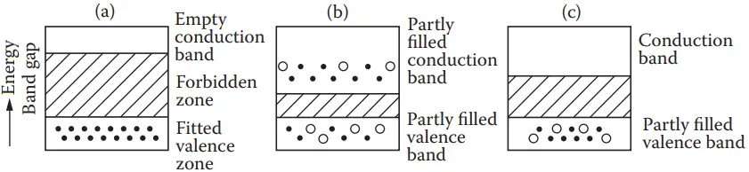
Since electrons in the outermost band of an atom determine how an atom will react or join with a neighboring atom, the outermost band is called the valence band. Some electrons in the valence band may be so energetic that they jump into a still higher band and are so far removed from the nucleus that a small amount of impressed force would cause them to move away from the atom. Such electrons are responsible for the conduction of heat and electricity, and this remote band is called a conduction band.
The difference in the energy of an electron in the valence band and the innermost subshell of the conduction band is called the band gap, or the forbidden gap.
- Materials whose valence bands are full have very high band gaps (>3 eV). Such materials are called insulators.
- Materials, on the other hand, that have relatively empty valence bands and may have some electrons in the conduction band are good conductors. Metals fall in this category.
- Materials with valence bands partly filled have intermediate band gaps (≤3 eV). Such materials are called semiconductors (Figure 1).
Pure semiconductors are called intrinsic semiconductors, while semiconductors doped with very small amounts of impurities are called extrinsic semiconductors.
If the dopant material has more electrons in the valence band than the semiconductor, the doped material is called an n-type of semiconductor. Such a material seems to have excess electrons available for conduction even though the material is electronically neutral. For example, silicon has four electrons in the valence band. Atoms of pure silicon arrange themselves in such a way that, to form a stable structure, each atom shares two electrons with each neighboring atom with covalent bonds.
If phosphorus, which has five valence electrons (one more than Si), is introduced as an impurity in silicon, the doped material seems to have excess electrons even though it is electrically neutral. Such a doped material is called n-type silicon.
If, on the other hand, silicon is doped with boron, which has three valence electrons (one less than Si), there seems to be a positive hole (missing electrons) in the structure, even though the doped material is electrically neutral. Such material is called p-type silicon.
Thus, n- and p-type semiconductors make it easier for the electrons and holes, respectively, to move in the semiconductors.
P–N Junction
As explained earlier, an n-type material has some impurity atoms with more electrons than the rest of the semiconductor atoms. If those excess electrons are removed, the impurity atoms will fit more uniformly in the structure formed by the main semiconductor atoms; however, the atoms will be left with positive charges.
On the other hand, a p-type material has some impurity atoms with fewer electrons than the rest of the semiconductor atoms. Therefore, these atoms seem to have holes that could accommodate excess electrons even though the atoms are electrically neutral (Figure 2).
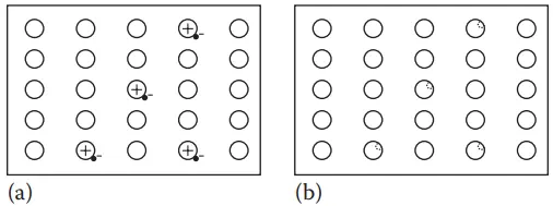
If additional electrons could be brought to fill the holes, the impurity atoms would fit more uniformly in the structure formed by the main semiconductor atoms; however, the atoms will be negatively charged.
The above scenario occurs at the junction when a p and an n type of material are joined together as shown in Figure 3.
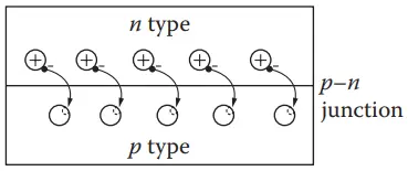
As soon as the two materials are joined, “excess” electrons from the n layer jump to fill the “holes” in the p layer. Therefore, close to the junction, the material has positive charges on the n side and negative charges on the p side. The negative charges on the p side restrict the movement of additional electrons from the n side to the p side, while the movement of additional electrons from the p side to the n side is made easier because of the positive charges at the junction on the n side.
This restriction makes the p–n junction behave like a diode. This diode character of a p–n junction is made use of in solar PV cells as explained in the following.
PV – Effect
When a photon of light is absorbed by a valence electron of an atom, the energy of the electron is increased by the amount of energy of the photon. If the energy of the photon is equal to or more than the band gap of the semiconductor, the electron with excess energy will jump into the conduction band where it can move freely.
If, however, the photon energy is less than the band gap, the electron will not have sufficient energy to jump into the conduction band.
In this case, the excess energy of the electrons is converted to excess kinetic energy of the electrons, which manifests in increased temperature. If the absorbed photon had more energy than the band gap, the excess energy over the band gap simply increases the kinetic energy of the electron.
It must be noted that a photon can free up only one electron even if the photon energy is a lot higher than the band gap. This fact is a big reason for the low conversion efficiency of PV devices.
The key to using the PV effect for generating useful power is to channel the free electrons through an external resistance before they recombine with the holes. This is achieved with the help of the p–n junction.
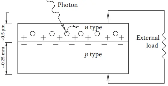
Figure 4 shows a schematic of a PV device. As free electrons are generated in the n layer by the action of photons, they can pass through an external circuit, recombine with positive holes in the lateral direction, or move toward the p layer. The negative charges in the p layer at the p–n junction restrict their movement in that direction.
If the n layer is made extremely thin, the movement of the electrons and, therefore, the probability of recombination within the n layer is greatly reduced unless the external circuit is open.
If the external circuit is open, the electrons generated by the action of photons eventually recombine with the holes, resulting in an increase in the temperature of the device.
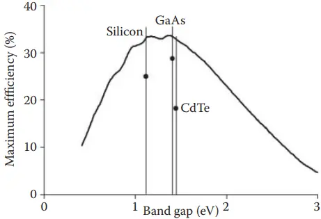
Efficiency of Solar Cells
Practical efficiency of a solar cell is much lower than that of theoretical efficiency. These efficiency limitations and the practical efficiencies of some of the cells are shown in Figure 5.
Some of the reasons for the actual efficiency being lower than the theoretical limitation are as follows:
- Reflection of light from the surface of the cell. This can be minimized by anti-reflection (AR) coating. For example, AR coatings can reduce the reflection from a Si cell to 3% from more than 30% from an untreated cell.
- Shading of the cell due to current collecting electrical contacts. This can be minimized by reducing the area of the contacts or making them transparent; however, both of these methods will increase the resistance of the cell to current flow.
- Internal electrical resistance of the cell.
- Recombination of electrons and holes before they can contribute to the current. This effect can be reduced in polycrystalline and amorphous cells by using hydrogen alloys.
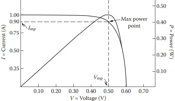
Maximum Power Point Tracking
It is important to ensure that the solar cells in a system are operating at the “maximum power point (MPP)” as seen in Figures 6.
There are several methods that can be used for maximum power point tracking (MPPT). They include simple methods (e.g., method of determining Vmp as equal to kVoc or determining Imp as equal to kIsc) as well as more involved methods (perturb and observe [P&O], incremental conductance [IC], artificial neural networks, and fuzzy logic methods).
Each method uses a DC – DC converter consisting of inductors and capacitors in a parallel circuit to measure the operating point of the cell and to change the output voltage to Vmp using a control algorithm. The parallel circuit consists of either a DC/DC single-ended primary inductor converter (SEPIC) or a buck – boost converter or a modification of these.
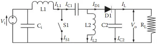
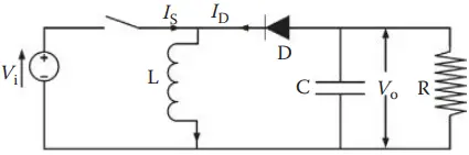
Figure 7 shows a schematic of a SEPIC converter and Figure 8 shows a schematic of a buck – boost converter. Opening and closing the switches allows the current to pass from the source through the inductor or from the capacitor to the load. The switching speed determines the output voltage seen by the load. The differences in the MPPT methods consist of how the Vmp is determined.
The simplest methods use a fixed constant “k” to determine it either from Voc or Isc. Both Voc and Isc change with insolation and the temperature of the cell and therefore will not always give the best values of Vmp.
The P&O method is much more accurate and more common in use. In a P&O algorithm, the output voltage is increased or decreased (perturbed) and the output power is compared with the power before perturbation. If the power increases (dP/dV > 0), then the voltage is increased more and vice versa. The method runs into problems if the insolation changes rapidly during a perturbation.
IC is a similar method in which current I and voltage V are measured before and after a perturbation and dI/dV is compared with I/V.
At MPP (dI/dV + I/V) = 0.
If the MPP is to the right of the perturbed point, then (dI/dV + I/V) > 0 and vice versa.
Design of a PV System
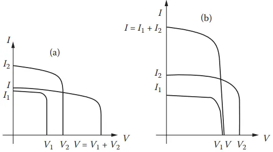
Solar cells may be connected in series, parallel, or both to obtain the required voltage and current. When similar cells or devices are connected in series, the output voltages and current are as shown in Figure 9. A parallel connection results in the addition of currents as shown in Figure 10. If the cells or devices 1 and 2 have dissimilar characteristics, the output characteristics will be as shown in Figure 11.
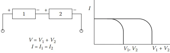
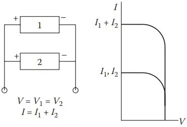
Cells are connected to form modules, modules are connected to form panels, and panels are connected to form arrays. Principles shown in Figures 9 and 10 apply to all of these connections
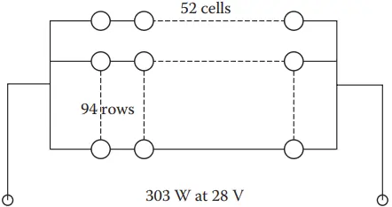
EXAMPLE : 1
An application requires 300 W at 28 V. Design a PV panel using solar cells if voltage and current from each cell are Vm = 0.542V, Im = 0.1143 A
Power/cell = 0.542 x 0.1143 = 0.062 W,
Number of cells required = 300/0.062 = 4840
Number of cells in series = System voltage/Voltage per cell = 28/0.542 = 52
Number of rows of 52 cells connected in parallel = 4840/52 ≈ 93.1
Since the number of rows must be a whole number, we may increase the number to 94 rows, which will give a 303 W output (Figure 12).
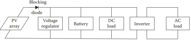
A blocking diode is used in series with a module or an array to prevent the current from flowing backward, for example, from the battery to the cells under dark conditions. A bypass diode is used in parallel with a module in an array to bypass the module if it is shaded. A PV system may be connected to a DC or an AC load as shown in Figure 13.
Design for Remote PV Applications
PV power may be ideal for a remote application requiring a few watts to hundreds of kilowatts of electrical power. Even where a conventional electrical grid is available, for some applications, where uninterruptible or emergency standby power is necessary, PV power would be appropriate.
Some examples of remote PV applications include water pumping for potable water supply and irrigation, power for remote houses, street lighting, battery charging, telephone and radio communication relay stations, and weather stations.
Examples of some other applications include electrical utility switching stations, peak electrical utility power where environmental quality is a concern, data acquisition systems, and specialty applications such as ventilation fans and vaccine refrigeration.
The design of a PV system is based on some basic considerations for the application.
- Which is more important, the daily energy output or the power (average or peak)?
- Is a backup energy source needed or available?
- Is energy storage important? What type—battery, pumped water, and so on?
- Is the power needed as AC or DC? What voltage?
There are three basic steps in the design of a PV system:
- Estimation of load and load profile
- Estimation of available solar radiation
- Design of PV system, including area of PV panels, selection of other components, and electrical system schematic.
Each of these steps will be explained in the following examples.
Estimation of Loads and Load Profiles
Precise estimation of loads and their timings (load profile) are important for PV systems since the system is sized as the minimum required to satisfy the demand over a day.
For example, if power is needed for five different appliances requiring 200, 300, 500, 1000, and 1500 W, respectively, so that only one appliance is on at any one time and each appliance is on for an average of 1 hour a day, the PV system would be sized based on 1500 W peak power and 3500 watt hours (Wh) of daily energy requirement.
The multiple loads on a PV system are intentionally staggered to use the smallest possible system, since the capital costs of a PV system are the most important as opposed to the energy costs in a conventional fuel-based system.
Estimation of Available Solar Radiation
If long-term measured solar radiation values are available at a location, then it is possible to estimate the average solar radiation per day. Otherwise, data for clear day can be used along with percent sunshine data (if available).
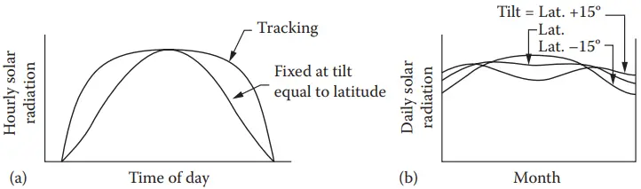
For designing a PV system, a decision is made whether the PV panel will be operated as tracking the sun or will be fixed at a certain tilt and azimuth angle.
For fixed panels, a tilt angle of latitude +15° works best for winter and latitude −15° works best for summer. To keep the panel fixed year round, an angle equal to the latitude provides the maximum yearly energy (see Figure 14).
PV System Sizing
If meeting the load at all times is not critical, PV systems are usually sized on the basis of the average values of energy and power needed, available solar radiation, and component efficiencies. This is known as the heuristic approach.
It is important to note that a system designed by this approach will not give the best design but may provide a good start for a detailed design. A detailed design accounts for the changes in the efficiencies of the components depending on the load and the solar radiation availability and whether the system is operating in a PV-to-load, PV-to-storage, or storage-to-load mode.
EXAMPLE : 2. Load calculations.
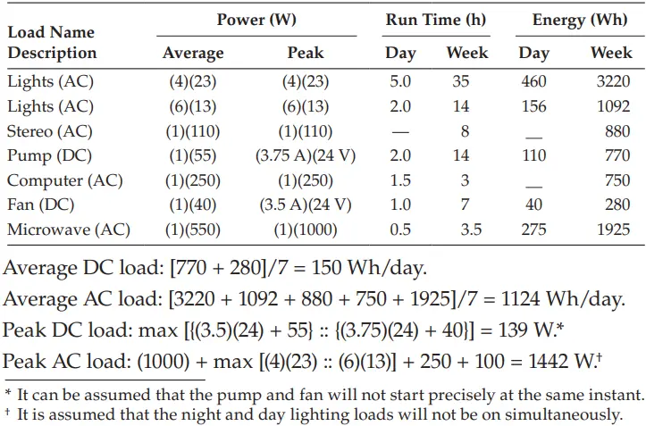
An owner of a remote cabin wants to install a PV power system. The loads in the home are described in the following. Assume that all lights and electronics are powered by AC. Find the daily and weekly peak and average energy use estimates. The system used is a 24V DC system with an inverter.
- Lights Four, 23W compact fluorescent bulbs. On at night for 5 h.
- Lights Six, 13W compact fluorescent bulbs. On for 2 h each (daytime).
- Stereo 110 W (amplifier), 15 W (other). On for 8 h per week.
- Water pump 55 W (3.75 amp start current). Runs for 2 h per day.
- Computer 250 W (monitor included). On for 1 1/2 h daily (weekend nights only)
- Bathroom fan 40 W (3.5 amp start current). On for 1 h per day.
- Microwave 550 W (AC) – 1000 W surge. On for 30 min per day.
SOLUTION : Loads need to be broken down according to (1) run time, (2) peak power, (3) night or day use, and (4) AC or DC loads. The load profile is as follows:
EXAMPLE: 3. Heuristic approach to PV system sizing.
A PV system using 50W, 12V panels with 6V, 125 Ah batteries is needed to power a home in Farmington, New Mexico, with a daily load of 1700 Wh. System voltage is 24 V. There is an average of 5 daylight hours in the winter. Specify the collector and storage values for the system using the heuristic approach.
SOLUTION
Load = 1700 Wh/day.
Daylight hours = 5 h/day.
Average panel output = 50 W.
Number of panels = 1700 / (5 x 50) = 6.8. , round off to 7 panels.
Since the system voltage is 24 V, but each panel produces only 12 V, an even number of panels will be needed. Therefore, the number of panels is equal to 8.
Farmington, New Mexico, is a very sunny location; thus, 3 days of storage is plenty. Assuming a battery efficiency of 75% and a maximum depth of discharge 70%,
Storage = (1700 x 3) / (0.75 × 0.7) = 9714 Wh
Number of batteries = 9714 / (125 × 6) = 13 (rounded off to the next whole number).
Since the system voltage is 24 V, and each battery provides 6 V, the number of batteries is increased to 16.
In a detailed design, the efficiencies of battery storage, inverter, and the balance of system (BOS) must be accounted for. The following example shows how these efficiencies increase the energy requirements of the PV panel.
EXAMPLE: 3. System operating efficiency.
Using the cabin electrical system from Example 2, calculate the overall system efficiency for each operating mode possible for the system. Estimate the amount of energy required per day for the system. When load timing (day or night), assume half of the load runs during the day and half runs at night.
The inverter used has an efficiency of 91%, the battery efficiency is 76%, and the distribution system efficiency is 96%.
SOLUTION : From the example, the loads are as follows:
Average DC load: 150 Wh/day,
Average AC load: 1124 Wh/day.
The various system efficiencies are as follows:
- PV to load (DC): 0.96 (day, DC),
- Battery to load (DC): (0.76)(0.96) = 0.73 (night, DC),
- PV to load (AC): (0.96)(0.91) = 0.874 (day, AC),
- Battery to load (AC): (0.76)(0.91)(0.96) = 0.664 (night/AC).
Expected day and night loads are as follows:
- Day (DC): (0.5)(110) + (0.5)(40) = 75 Wh/day,
- Night (DC): (0.5)(110) + (0.5)(40) = 75 Wh/day,
- Day (AC): (156) + (0.5)(880 + 750)/7 + (0.5)(275) = 409.9 Wh/day,
- Night (AC): (460) + (0.5)(880 + 750)/7 + (0.5)(275) = 713.9 Wh/day
Without considering system efficiency, the daily energy requirement is Eday = (150) + (1124) = 1274 Wh/day.
The expected daily energy requirement is
Eday = (75/0.96) + (75/0.73) + (409.9/0.874) + (713.9/0.664)
Eday = 1725 Wh/day
The actual energy requirement is 35% higher than simple calculation.