Varactor Diode
The varactor diode is a semiconductor, voltage-dependent variable capacitor alternatively known as varicap or voltacap or voltage-variable capacitor (VVC) diode. Basically, it is just a reverse-biased junction diode whose mode of operation depends on its transition capacitance (CT).
We know that the reverse-biased junctions behave like capacitors whose capacitance is ∝ 1/VRn where n varies from 1/3 to 1/2. As reverse voltage VR is increased, depletion layer widens thereby decreasing the junction capacitance. Hence, we can change diode capacitance by simply changing VR.
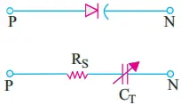
Silicon diodes which are optimised for this variable capacitance effect are called varactors. The picture, schematic symbol and a simple equivalent circuit for a varactor are shown in Fig. 1.
Varactors may be of two types as shown in Fig. 2. The doping profile of the abrupt-junction diode is shown in Fig. 2(a) and that of the hyperabrupt-junction diode in Fig. 2(b).
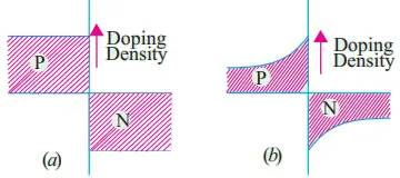
The abrupt-junction diode has uniform doping and a capacitive tuning ratio (TR) of 4:1. For example, if its maximum transition capacitance is 100 pF and minimum 25 pF, then its TR is 4:1 which is not enough to tune a broadcast receiver over its entire frequency range of 550 to 1050 kHz.
The hyperabrupt-junction diode has highest impurity concentration near the junction. It results in narrower depletion layer and larger capacitance. Also, changes in VR produce larger capacitance changes. Such a diode has a tuning range of 10:1 enough to tune a broadcast receiver through its frequency range of nearly 3:1.
Applications: Since the junction capacitance of a varactor is in the pF range, it is suitable for use in high-frequency circuits. Its main applications are as
- automatic frequency control device,
- FM modulator,
- adjustable band-pass filter,
- parametric amplifier.
PIN Diode
Construction: It is composed of three sections. These are the usual P and N-regions but sandwiched between them is an intrinsic layer or I-layer of pure silicon (Fig. 3). Being intrinsic (or undoped) layer, it offers relatively high resistance. This high-resistance region gives it two advantages as compared to an ordinary P-N diode.

The advantages are:-
- decrease in capacitance Cpn because capacitance is inversely proportional to the separation of P-and N-regions. It allows the diode a faster response time. Hence, PIN diodes are used at high frequencies (more than 300 MHz);
- possibility of greater electric field between the P-and N-junctions. It enhances the electron-hole pair generation thereby enabling PIN diode to process even very weak input signals.
Diode Resistance:
- When forward-biased, it offers a variable resistance rac ≅ 50/I where I is the dc current in mA. For large dc currents, it would look like a short.
- When reverse-biased, it looks like an ‘open’ i.e. it offers infinite resistance in the reverse direction.
Operation: Its use in electronic high frequency switching is illustrated in Fig. 4. When the diode is reverse-biased, it looks like an ‘open’ as shown in Fig. 4(b). The 500-MHz input signal voltage divides across the series-connected 100 Ω resistance and the diode in proportion to their resistances.
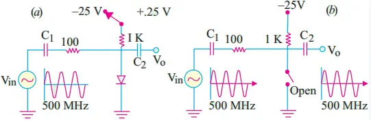
Since the diode has infinite resistance (being open), the entire input signal appears across it. Hence, the whole input signal passes out via coupling capacitor C2 without any attenuation (or loss).
When the diode is forward-biased by the + 25 V dc source, I = 25/1K = 25 mA. Hence, diode resistance rac = 50/25 = 2 Ω as shown by its equivalent circuit in Fig. 5.
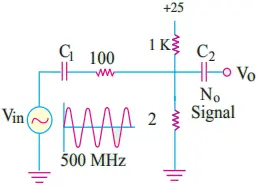
Now, almost all the input signal voltage drops across 100 Ω resistance and practically none across the 2 Ω resistance. Hence, there is hardly any signal output.
In practice instead of mechanically switching the diode-biasing supply from − 25 V to + 25 V, a transistor is used to do this switching operation.
In this way, we can turn a very high frequency signal (MHz range) OFF and ON with the speed of a transistor switching circuit.
Applications:
- as a switching diode for signal frequencies upto GHz range;
- as an AM modulator of very high frequency signals.
Schottky Diode
It is also called Schottky barrier diode or hot-carrier diode. It is mainly used as a rectifier at signal frequencies exceeding 300 MHz. It has more uniform junction region and is more rugged than PIN diode − its main rival.
Construction: It is a metal-semiconductor junction diode with no depletion layer. It uses a metal (like gold, silver, platinum, tungsten etc.) on the side of the junction and usually an N-type doped silicon semiconductor on the other side.
Operation: When the diode is unbiased, electrons on the N-side have lower energy levels than electrons in the metal. Hence, they cannot surmount the junction barrier (called Schottky barrier) for going over to the metal.
When the diode is forward-biased, conduction electrons on N-side gain enough energy to cross the junction and enter the metal. Since these electrons plunge into the metal with very large energy, they are commonly called ‘hot-carriers’. That is why this diode is often referred to as hot-carrier diode.
Applications: This diode possesses two unique features as compared to an ordinary P-N junction diode:
- it is a unipolar device because it has electrons as majority carriers on both sides of the junction. An ordinary P-N junction diode is a bipolar device because it has both electrons and holes as majority carriers;
- since no holes are available in metal, there is no depletion layer or stored charges to worry about. Hence, Schottky diode can switch OFF faster than a bipolar diode.
Because of these qualities, Schottky diode can easily rectify signals of frequencies exceeding 300 MHz. It can produce an almost perfect half-wave rectified output. The present maximum current rating of the device is about 100 A. It is commonly used in switching power supplies that operate at frequencies of 20 GHz.
Another big advantage of this diode is its low noise figure which is extremely important in communication receivers and radar units etc. It is also used in clipping and clamping circuits, computer gating, mixing and detecting networks used is communication systems.
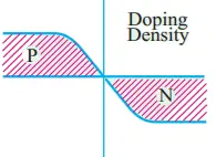
Step Recovery Diode
It is another type of VVC diode having a graded doping profile where doping density decreases near the junction as shown in Fig. 6. This results in the production of strong electric fields on both sides of the junction.
Theory: At low frequencies, an ordinary diode acts as a rectifier. It conducts in the forward direction but not in the reverse direction i.e. it recovers immediately from ON state to the OFF state.
However, it is found that when driven forward-to-reverse by a high-frequency signal (above a few MHz), the diode does not recover immediately. Even during the negative half-cycle of the input signal when the diode is reverse-biased, it keeps conducting for a while after which the reverse current ceases abruptly in one step.
This reverse conduction is due to the fact that charges stored in the depletion layer during the period of forward bias take time to drain away from the junction.
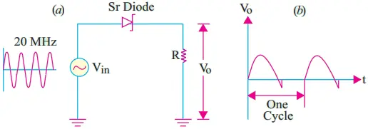
Fig. 7(a) shows a step-recovery diode being driven by a 20-MHz signal source. As seen from Fig. 7(b), it conducts in the forward direction like any diode.
During the reverse half-cycle, we get reverse current due to the draining of the stored charge after which current suddenly drops to zero. It looks as though diode has suddenly snapped open during the early part of the reverse cycle.
That is why it is sometimes called a snap diode. The step or sudden recovery from reverse current ON to reverse current OFF gives the diode its name.
Applications: Its main use is in high-frequency harmonic generator circuits as a frequency multiplier as explained below. It is found that whenever a waveform has sudden step or transition, it contains all the harmonics of the input signal (i.e. multiples of its fundamental frequency).
Fig. 8 shows how the output of a step recovery diode can be used to drive a tuning circuit which can be made to tune out all harmonics except one i.e. fifth in this case (100 MHz). With an input signal of 20 MHz, the step recovery diode generates harmonics of different multiple frequencies listed above. However, the resonant L-C circuit is tuned to 5th harmonic of f = 100 MHz.
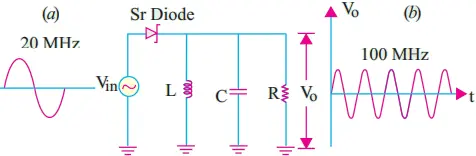
Hence, all except this harmonic are filtered out of the circuit. The signal appearing across R is almost a pure sine wave with f = 100 MHz as shown separately in Fig. 8(b).
Step-recovery diodes are also used in pulse and digital circuits for generating very fast pulses with rise time of less than 1 nanosecond.
Gunn Diode
It is a negative-resistance microwave device for oscillator applications. As shown in Fig. 9, it consists of a thin slice of N-type gallium arsenide sandwiched between two metal conductors.
The central section is N-gallium arsenide whereas the two outer sections are epitaxially grown from GaAs with increased doping and higher conductivity.
As an oscillator, its frequencies range from 5 GHz and 100 mW output upto 35 GHz and 1 mW output. Efficiencies of 3 to 5 per cent are possible at present.
IMPATT Diode
IMPATT stands for impact avalanche and transit time diode. As the name indicates, it is a microwave diode that utilizes the delay time required for attaining an avalanche condition plus transit time to produce a negative-resistance characteristic. It is used as a microwave oscillator within a frequency range of 10 – 100 GHz.