Memory is an electronic component with the function of “memory”, which uses physical devices with two stable states to store information. The main function of the memory is to store the program and various data, and can be in the process of computer operation at high speed, automatically complete the program or data access.
In this article, we will introduce the composition of the memory components, as well as the working principle of the memory related knowledge, specifically to see:
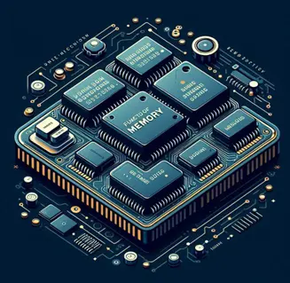
Structure of Memory Components
In computer systems, a three-level memory structure is usually adopted, that is, a structure composed of cache memory, main memory and external memory. The memory that the CPU can directly access is called internal memory, which includes cache memory and main memory. The CPU cannot directly access the external memory. The information of the external memory must be transferred to the internal memory before it can be processed by the CPU.
1. Cache memory
Also known as fast cache memory, referred to as fast memory. It is a high-speed, small-capacity memory in the computer system. It temporarily stores instructions and data and is a copy of the main memory content. It can directly exchange data and instructions with the CPU. At present, it is mainly composed of bipolar semiconductor memory, which has a fast access speed but a small storage capacity.
2. Main memory
The main memory is the main memory of the computer system. Used to store a large amount of programs and data during computer operation. Exchanges data and instructions with fast cache memory. Also exchanges data with external memory. Currently, it is generally composed of MOS memory.
3. External memory
Also called auxiliary memory, referred to as external memory. It is composed of magnetic surface memory. At present, disk memory and tape memory are mainly used. The characteristics are large storage capacity, but slow access speed. It is usually used to store system programs and large data files and databases.
Working Principle of Memory
Here we only introduce the working principle of dynamic memory (DRAM). Each dynamic memory has only one input data line and only 8 address pins. In order to form a 64K address, an address formation circuit must be specially designed between the system address bus and the chip address lead. The system address bus signal can be added to the 8 address pins in time-sharing, and the storage unit in the chip is selected with the help of the row latch, column latch and decoding circuit inside the chip. The latch signal is also generated by the external address circuit.
When data is to be read from the DRAM chip, the CPU first adds the row address to A0 – A7, and then sends the RAS latch signal. The falling edge of the signal latches the address inside the chip. Then the column address is added to A0 – A7 of the chip, and then the CAS latch signal is sent. The column address is also latched inside the chip at the falling edge of the signal. Then keep WE=1, and the data is output and maintained during the effective period of CAS.
When data needs to be written into the chip, the row and column addresses latch RAS and CAS in the chip in turn, and then WE is effective, plus the data to be written, and the data is written into the selected storage unit.
Since the capacitor cannot keep the charge unchanged for a long time, it is necessary to perform a reread operation on each storage unit of the dynamic storage circuit regularly to keep the charge stable. This process is called dynamic memory refresh. The refresh of DRAM in PC/XT machines is implemented using DMA. First, the counter 1 of the programmable timer 8253 is used to generate a DMA request every 15 – 12 µs, which is added to the 0 channel of the DMA controller. When the request of DMA controller channel 0 is responded, the DMA controller sends a refresh address signal to perform a read operation on the dynamic memory, refreshing one row each time it reads.