Metal-oxide semiconductor field effect transistors (MOSFETs) are the other family of transistors that are commonly used. The MOSFET is based on the original field effect transistor (FET) that was introduced in the 1960s. Similar to the BJT family, they are also three terminal devices, but they have different names for the terminals, and they operate differently.
The three terminals are the gate (similar to base), drain (similar to collector), and source (similar to emitter). The naming of the terminals comes from the flow of electrons between the source and drain when the transistor is conducting.

MOSFET
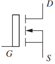
The most commonly used MOSFET is the enhanced type and is available as n- or p-type. We will limit the discussion to the n-type enhanced MOSFET here. Figure 1 shows the symbol of the n-type MOSFET.
MOSFET Basics
The voltage applied to the gate (or the electric field) is the signal that controls the operation of the transistor and hence the name field effect transistor. This is in contrast to a BJT where the current applied to the base controls its operation.
The gate is insulated from the drain-source circuit. This is indicated in the symbol by the separation of the gate terminal from the drain-source connection. The gate has a very high internal resistance (RGate = ∼1014 Ω), such that almost no current flows into the gate.
This insulation makes it easy to analyze MOSFET circuits, because the gate circuit can be analyzed separately from the drain-source circuit. In addition, the high input resistance means that the gate draws no current except for a small leakage current in the nanoampere range.
The high-input impedance of a MOSFET gives it an advantage in interfacing with other logic circuits.
MOSFETs have three states: cutoff, active, and saturation, which are similar to BJTs. MOSFETs have a higher power rating and generate less heat than BJTs.
They act as voltage-controlled resistors. When the transistor is OFF, the drain-source resistance is very high, and when the transistor is fully ON, the drain-source resistance is very low (can be less than 1 Ω).
When the transistor is ON, current flows from the drain to the source (electrons travel in the opposite direction).
n-type enhancement MOSFETs operate with a positive voltage applied to the gate.
Performance Characteristics of MOSFETs
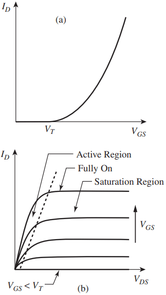
The transfer and output characteristics of MOSFET are shown in Figure 2.

(b) output characteristics of a
MOSFET
Figure 2(a) shows the relationship between the drain current (ID) and the voltage between the gate and the source (VGS). The figure shows that the drain current is zero until VGS exceeds the threshold voltage (VT) for the MOSFET.
- When VGS < VT, the MOSFET is said to be in the cutoff or non-conducting state.
The threshold voltage for normal MOSFETs (such as 2N4351) is between 2 to 5 V, while for logic-level MOSFETs (ones that are designed to be driven directly from outputs of logic gates, such as microcontrollers) the threshold voltage is about 0.3 to 1.0 V.
- As VGS increases above VT, the drain current increases.
Figure 2(b) shows the relationship between the drain current and the voltage between the source and the drain (VDS) for different values of VGS.
- For a given VGS > VT, the drain current increases with VDS for a small VDS. This is called the active or ohmic region, where the MOSFET acts like a variable resistor whose resistance is controlled by VGS.
- However, as VDS increases, the drain current levels off and stays constant. This is called the saturation region, where the drain current value is independent of VDS.
- When VGS is significantly higher than the threshold voltage (approximately 10 V for a normal MOSFET), the transistor is said to be in the fully ON state where the drain current is maximum.

driving a motor.
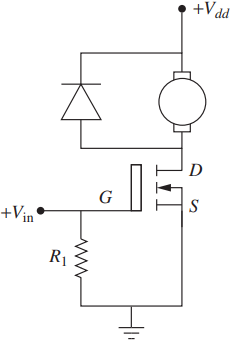
MOSFETs are typically used for switching applications (ON/OFF) to drive motors or LEDs. A typical circuit is shown in Figure 3.
When the transistor is OFF, no current flows from the drain to the source, and the motor is OFF. When the transistor is fully ON, current flows to the motor, and the motor is ON.
Note the use of the flyback diode in the circuit to protect the transistor from the large voltage build-up that occurs when the transistor is switched off.
The resistor at the input is used to drive the gate input to ground and completely turns OFF the transistor when the input voltage is zero.
Performance Parameters of MOSFETs
| Part Number | On Resistance Rds (ON) | Max. Drain Current ID (max) | Power Dissipation Pd | Gate Threshold Voltage VGS(th) | Drain-to- Source Breakdown Voltage Vdss |
| 2N4351 | <= 300 Ω | 100 mA | 375 mW | 1 – 5 V | >= 25 V |
| NTE2980 | 0.2 – 0.28 Ω | 6.7A (VGS = 5 V) | 25 W | 1 – 2 V | >= 60 V |
| IRFZ14 | 0.2 Ω | 10 A | 43 W | 2 – 4 V | >= 60 V |
Some of the parameters of a logic-level MOSFET (NTE2980), normal MOSFET (2N4351), and a Power MOSFET (IRFZ14) are shown in above Table. These parameters are defined here.
Rds(ON): The resistance between the drain and source terminals when the MOSET is fully turned ON.
ID(max): The maximum current between the drain and source that can be passed by the transistor. It is a function of Rds(on) and the package type of the transistor
Pd: The power dissipation rating for the transistor.
VGS(th): The minimum voltage between the gate and the source that causes the transistor to start conducting.
Vdss: The maximum voltage between the drain and source when the transistor is OFF.
Power Handling Capacity of MOSFET
Similar to BJTs, the power-handling capacity of MOSFET transistors is a very important consideration in the selection of these components. When the power to be dissipated is above 1 W, the MOSFET is mounted on a heat sink. In these MOSFETs, the package has a metal tab which is mounted against the heat sink.
The dissipated power in a MOSFET is the product of the drain current and the voltage across the transistor. Since the voltage across the transistor is equal to the product of current and the resistance, the power is then given by
Pd = I2D Rds(on)
when the transistor is fully conducting.