MOSFET stands for metal oxide semiconductor field effect transistor. It is also called IGFET or insulated gate field effect transistor. It is an integrated circuit (IC) or a semiconductor chip. It is fabricated by VSLI using planar technology. The thickness of SiO2 layer is 1000 to 2000 Ao.
The larger input resistance of the MOSFET is due to the SiO2 layer. It is a voltage controlled device which is symmetrical as the source and drain can be interchanged. MOSFETs are widely used as switches in digital circuits.
Some advantages of MOSFETs over BJT and JFET are:
- The layout area of MOSFET is less than the area for BJT.
- It consumes very less power.
- Noise immunity of MOSFET is larger than that of BJT.
- Scaling of MOSFET is possible.
- MOSFET is faster than JFET.
MOSFETs are divided into following two types, based on their construction and mode of operation.
- Enhancement type (EMOSFET)
- Depletion type (DMOSFET)
Both these types can further be p- and n-channel type depending on whether the channel is made up of nor p-type semiconductor. The channel is also called as the inversion layer.
For n-channel MOSFET (NMOS), the substrate is p-type and for a p-channel MOSFET (PMOS) it is n-type.
Depletion Type MOSFETs
Depletion type MOSFETs have a pre-existing/diffused channel between the drain and the source terminals. These are further classified as n-channel and p-channel DMOSFETs based on whether the channel material is n- or p-type semiconductor respectively.
The n-channel MOSFET is also sometime called dual MOSFET because it is suitable to operate in both the depletion mode and enhancement mode. However, p-channel DMOSFET is more popular for enhancement operations.
The operation of NMOS is faster than that of PMOS because of greater mobility of neutrons (µn) in comparison to protons (µp).
PMOS is easier to fabricate but it is bulky. For the same application, to get the equal performance between the two types of DMOSFETs, PMOS requires twice the area of NMOS. Thus NMOS has higher package density.
Depletion Type n-channel MOSFET
Figures 1(a) and (b) show the cross-sectional view and circuit symbols n-channel depletion MOSFET, respectively. It is constituted by a substrate made of p-type semiconductor material and two n+ type regions linked by diffused n-channel present on it.
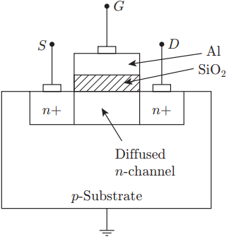
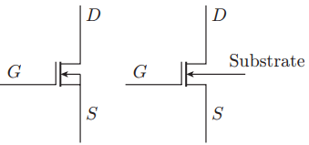
The drain and source terminals are connected by metal contacts and the gate terminal is connected through insulating SiO2 layer present on the top of the n-channel.
The MOSFET acts as a capacitor which is formed at the gate section with Al plate. The channel act as two plates of the capacitor and SiO2 acts as the dielectric material.
The operation of n-channel depletion type MOSFET can be considered under two modes (i) depletion and (ii) enhancement, depending on if the negative charge carriers moving towards the drain are depleted or enhanced under the applied gate-source voltage.
Depletion Mode Operation of N-Channel MOSFET
The construction and operation in depletion mode are depicted in Fig. 2. The drain is positively biased with respect to source and to operate under depletion mode the gate is negatively biased with respect to source.
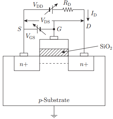
1. When no gate-source voltage is applied, that is when the gate and source terminals are shorted, (VGS = 0) and a positive voltage is applied between the drain and the source (VDS > 0), then current (ID) flows through the n-channel by the flow of electrons towards the drain at positive potential.
The current increases with increase in value of VDS and becomes constant for a certain value of VDS.
Here the maximum negative charges (electrons) will be moving from source to drain and therefore the drain current is maximum and is given by IDSS (drain to source saturation current).
2. When a negative voltage is applied to gate, that is VGS < 0, then the drain current decreases with increase in negative gate-source potential.
This is because the electrons are repelled towards the p-channel substrate where they recombine with holes, thus reducing the number of free electrons reaching the drain and drain current is reduced.
When gate is given sufficiently more negative voltage, a large number of positive charges will be created in the channel and this will result a total recombination so that no negative charge will be reaching the drain end and ID reduces to zero. Now the channel is cut-off.
This is known as the depletion mode of operation.
These drain and transfer characteristics under the depletion mode of operation are shown in Fig. 3(a) and (b).
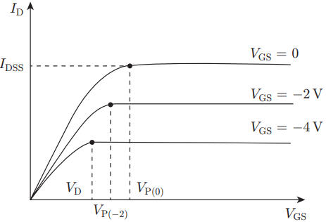
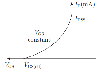
The equation for drain current in depletion n-channel MOSFET is

Here VP is the pinch-off voltage, where channel thickness is zero at drain end and current becomes constant. The polarity of VP and VGS is the same and the drain current decreases as a parabolic variation with VGS.
Enhancement Mode Operation N-Channel MOSFET
Now consider the operation of n-channel MOSFET under the enhancement mode. Here the drain is positively biased with respect to the source and to operate under enhancement mode, gate is also positively biased with respect to source (Fig. 4). In this mode of operation, the applied gate to source voltage increases the majority carriers of the channel.
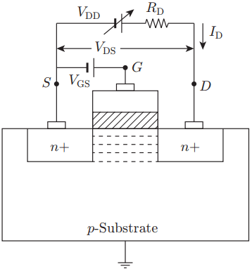
1. When VGS = 0, the voltage is zero and therefore inversion charge is zero and therefore minimum number of negative charges will be moving from source to drain. The drain current is minimum and is denoted by IDSS (drain to source saturation current).
2. When a positive voltage is applied to gate, that is VGS > 0, there is a positive gate-source potential. Therefore negative charges are created in the channel and this will increase the number of negative charges to drain. Thus ID increases to value greater than IDSS. ID further increases with increase in positive voltage applied to the gate.
The drain and transfer characteristics under the enhancement mode of operations are shown in Figs. 5(a) and (b).
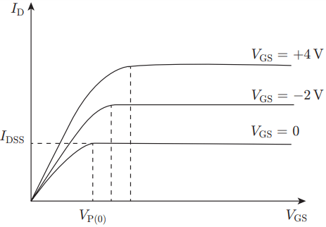
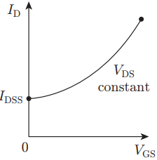
Here VP(0) is the minimum pinch-off voltage.

Under pinch-off mode of conduction; VDS = VGS + VP
The drain current is given by
VGS and VP must have opposite polarity.
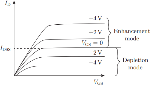
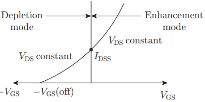
The overall output and transfer characteristic curves for for n-channel depletion MOSFET in depletion and enhancement mode are as shown in Fig. 6(a) and (b).
Important points:
- In the depletion MOSFET channel is, diffused channel.
- In depletion MOSFET if VGS is kept zero then ID = IDSS.
Depletion Type p-Channel MOSFET
The construction of the p-channel depletion type MOSFET is similar to that of n-channel depletion MOSFET as shown in Fig. 7(a).
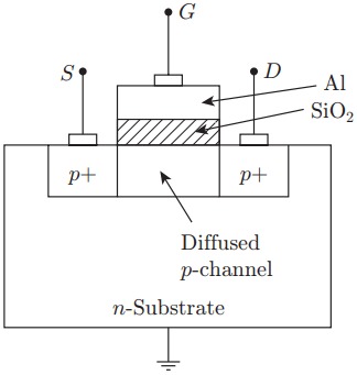
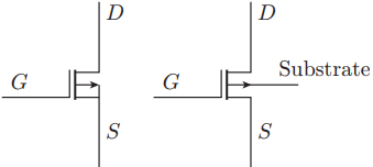
It comprises a substrate made of n-type semiconductor material and two p+ regions which are connected to source and drain terminals by metal contacts. The circuit symbols for this MOSFET are shown in Fig. 7(b).