The insulated gate bipolar transistor (IGBT) combines the advantageous features of MOSFET (such as voltage control, fast switching) and BJT (such as low ON-state losses and high OFF-state voltage capability. These devices have near ideal characteristics for high voltage (>100V) and medium frequency (<20 kHz) applications.
The IGBT is a three terminal device with
- emitter lead E (similar to emitter E of BJT),
- collector lead C (similar to collector of BJT) and
- a gate lead G (similar to gate of MOSFET).
Like the MOSFET it is a voltage controlled device where the flow of current from the collector to the emitter is controlled by the voltage applied between the gate-emitter terminals.
Construction of IGBT
The cross-sectional view of a n-channel IGBT is depicted in Fig. 1.
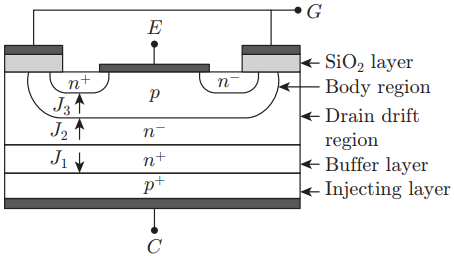
It consists of four layers p- and n-type semiconductors. The gate is connected to a metallic conductor and is insulated from the bulk of the IGBT by silicon oxide layer acting as an insulator.
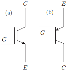
The circuit symbols of p- and n-type IGBTs are given in Figs. 2(a) and (b), respectively In the constructional view of an IGBT, as shown in Fig. 1, the major difference with a corresponding MOSFET cell structure lies in the inclusion of an additional p+ injecting layer, forming a p-n junction with the drain layer to inject minority carriers into the same.
The n-type drain layer itself has two different doping levels, the lightly doped n− region which is called the drain drift region and the heavily doped n+ region known as the buffer layer.
Doping level and width of the buffer layer sets the forward blocking voltage of J2 or the reverse breakdown voltage of the device. However, the doping level or the reverse breakdown voltage does not affect the on state voltage drop of the device. This type of construction of the device is called punch trough or PT design.
The non-punch through or NPT type of construction can also be made without the added n+ buffer layer.
The PT type of construction of the device offers lower on state voltage drop compared to the NPT type construction generally for the devices having lower voltage ratings.
However, the reverse breakdown voltage for the device is lowered as a result, since the reverse breakdown voltage of the junction J1 between the buffer and the injecting p+ – layer is small.
Operation of IGBT
The IGBT can be viewed as equivalent to a MOSFET with a diode connected to its drain or as combination of a MOSFET and a PNP transistor.
It behaves essentially as a MOSFET when considered from the input perspective with three terminals, collector, emitter and gate.
When the gate-emitter voltage is less than the minimum threshold voltage, no inversion layer is formed in the p-type body region and the device is in the OFF state due to negligible current through the collector. Only very small leakage current flows through the device between the collector and emitter under this condition.
The forward voltage applied between the collector and the emitter drops almost entirely across the junction J2 as shown in Fig. 1.
When the gate to emitter voltage is increased to exceed the threshold value, an inversion layer is formed in the p-type body region under the gate. This inversion layer or channel shorts the emitter and the drain drift layer, resulting in an electron current flowing from the emitter through this channel to the drain drift region.
This causes substantial hole injection from the p+ type collector to the drain drift region and a portion of these holes recombine with the electrons coming to the drain drift region through the channel.
The rest of the holes cross the drift region and reach the p-type body, to be collected by the source metallisation.
The total ON-state voltage drop occurring across an IGBT when under conduction has three components, which are listed as follows.
- The voltage drop across junction J1 which follows the already known exponential law of a p-n junction.
- The voltage drop due to the resistance of the drain drift region arising due to the strong conductivity modulation by the injected minority carriers from the collector, this component is considerably lower as compared to that in a MOSFET and contributes to the reduced conduction voltage drop across an IGBT in comparison to a MOSFET of equivalent rating.
- The voltage drop across due to the channel resistance, which has a magnitude almost equal to that of a MOSFET of comparable rating.
Static Characteristics of IGBT
The V-I characteristics of an n-channel IGBT are shown in Fig. 3 along with the circuit configuration.
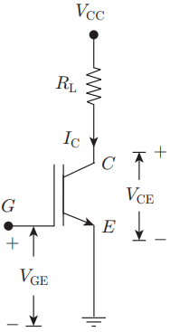
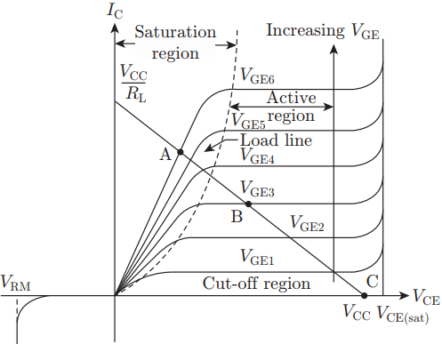
The characteristics shows the plot of collector current IC versus VCE for increasing gate-emitter voltage VGE.
When the applied gate emitter voltage (VGE) is below the threshold value, only a very small leakage current flows though the device and the collector-emitter voltage almost equals the supply voltage as depicted by point A in Fig. 3. The device is considered in OFF mode under this condition and is operating in the cut off region.
The maximum forward voltage that the device can withstand in this mode is VCES and this voltage is determined by the avalanche breakdown voltage of the body-drain p-n junction. This breakdown voltage is independent of the collector current unlike in a BJT.
IGBTs with non-punch through type design can block a maximum reverse voltage known as VRM equal to VCES in the cut-off mode. On the other hand, for punch through design of IGBTs, VRM is negligible ranging to only a few tens of volts due to the presence of the heavily doped n+ drain buffer layer.
As the gate emitter voltage VGE is increased beyond the threshold value, the IGBT enters into the active region of operation where the collector current IC is determined by the transfer characteristics of the device as shown in Fig. 3. This characteristic is similar to that of a power MOSFET and is reasonably linear over most of the collector current range.
The ratio of IC to (VGB — VGE(th)) is called the forward trans-conductance (gFE) of the device and is an important parameter in the gate drive circuit design.
Performance Parameters of IGBT
Generally the power electronic converters employ switching devices which can distort the input current from the sinusoidal nature. This distorted input current injects harmonics to the source. To measure this distortion some performance parameters and their individual standards are set.
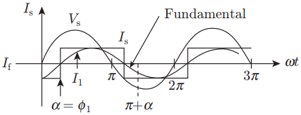
To discuss these consider the waveform for a single phase converter as shown in Fig. 4, where Vs and Is are of source voltage and current, respectively and V1 and I1 are fundamental components of source voltage and current.
Also value of input rms voltage Vrms = Vs as both are the same, considering the case of single phase fully controlled rectifier feeding a heavily inductive load to get flat load current.
1. Input power factor: It is defined as the radio of the input mean power to rms apparent power. Thus input power factor (PF or pf) is given by
PF = = Mean power ÷ Vrms Irms = Mean power ÷ Vs Is
The input voltage is sinusoidal thus the input mean power is defined as Vs I1 cosɸ1 where as defined Vs is the rms value of input voltage and I1rms is the rms value of fundamental current and f1 is the angle between the input voltage and fundamental current. Then
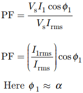
2. Displacement factor: It is defined as the cosine of the angle between source voltage and fundamental input current. Thus,
Displacement factor = cosɸ1
3. Distortion factor: It is defined as the ratio of fundamental component of rms value input current to rms value of total input current. Thus,
Distortion factor = I1rms ÷ Irms
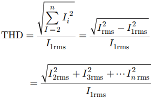
4. Total harmonic distortion (THD): This is defined as the ratio of rms value harmonic component of input current to the rms value of fundamental component input current. Thus,
5. Crest factor: It is the ratio of peak value of input emf to its rms value.
Thus, CF(or c) = Imax ÷ Irms
6. Ripple factor: It is the ratio of rms value ac component of input current to the average value of input emf. Thus,

7. Form factor: It is the ratio of rms value to average value of input current.
Thus, FF(or ) F = Irms ÷ Iavg
Based on the above relation, the RF can be again defined as

Related Posts
- Operation of Thyristors
- Static Characteristics of SCR | Thyristor
- Silicon Controlled Rectifier Function
- Applications & Characteristics of SCR
- SCR Selection Criteria
- Thyristor | SCR Specifications and Ratings
- Operation of Triac & GTO
- Triac Working
- Characteristics, Operation, & Construction of IGBT
- Freewheeling Diode in Controlled Rectifier
- Reverse Recovery Characteristics of Power Diode