Reverse Recovery Characteristics of Power Diode
Ideally, a diode should have no reverse recovery time. However, the manufacturing cost of such a diode may increase. In many applications, the effects of reverse recovery time is not significant, and inexpensive diodes can be used.
Depending on the recovery characteristics and manufacturing techniques, the power diodes can be classified into the following three categories:
- Standard or general-purpose diodes
- Fast-recovery diodes
- Schottky diodes
General-purpose diodes are available up to 6000 V, 4500 A, and the rating of fast-recovery diodes can go up to 6000 V, 1100 A. The reverse recovery time varies between 0.1μs and 5μs. The fast-recovery diodes are essential for high-frequency switching of power converters.
Schottky diodes have a low on-state voltage and a very small recovery time, typically in nanoseconds. The leakage current increases with the voltage rating and their ratings are limited to 100 V, 300 A.
A diode conducts when its anode voltage is higher than that of the cathode; and the forward voltage drop of a power diode is very low, typically 0.5 V to 1.2 V. The characteristics and practical limitations of these types restrict their applications.
General-Purpose Diodes
The general-purpose rectifier diodes have relatively high reverse recovery time, typically 25μs; and are used in low-speed applications, where recovery time is not critical (e.g., diode rectifiers and converters for a low-input frequency up to 1-kHz applications and line-commutated converters).
These diodes cover current ratings from less than 1 A to several thousands of amperes, with voltage ratings from 50 V to around 5 kV. These diodes are generally manufactured by diffusion.
However, alloyed types of rectifiers that are used in welding power supplies are most cost-effective and rugged, and their ratings can go up to 1500 V, 400 A.
Fast-Recovery Diodes
The fast-recovery diodes have low recovery time, normally less than 5μs. They are used in dc–dc and dc–ac converter circuits, where the speed of recovery is often of critical importance. These diodes cover current ratings of voltage from 50 V to around 3 kV, and from less than 1 A to hundreds of amperes.
For voltage ratings above 400 V, fast-recovery diodes are generally made by diffusion and the recovery time is controlled by platinum or gold diffusion.
For voltage ratings below 400 V, epitaxial diodes provide faster switching speeds than those of diffused diodes. The epitaxial diodes have a narrow base width, resulting in a fast recovery time of as low as 50 ns.
Schottky Diodes
The charge storage problem of a pn-junction can be eliminated (or minimized) in a Schottky diode. It is accomplished by setting up a “barrier potential” with a contact between a metal and a semiconductor.
A layer of metal is deposited on a thin epitaxial layer of n-type silicon. The potential barrier simulates the behavior of a pn-junction. The rectifying action depends on the majority carriers only, and as a result there are no excess minority carriers to recombine. The recovery effect is due solely to the self-capacitance of the semiconductor junction.
The recovered charge of a Schottky diode is much less than that of an equivalent pn junction diode. Because it is due only to the junction capacitance, it islargely independent of the reverse di/dt.
A Schottky diode has a relatively low forward voltage drop. The leakage current of a Schottky diode is higher than that of a pn-junction diode.
A Schottky diode with relatively low-conduction voltage has relatively high leakage current, and vice versa. As a result, the maximum allowable voltage of this diode is generally limited to 100 V. The current ratings of Schottky diodes vary from 1 to 400 A.
The Schottky diodes are ideal for high-current and low-voltage dc power supplies. However, these diodes are also used in low-current power supplies for increased efficiency.
Silicon Carbide Diodes
Silicon carbide (SiC) is a new material for power electronics. Its physical properties outperform Si and GaAs by far.
For example, the Schottky SiC diodes manufactured by Infineon Technologies have ultralow power losses and high reliability. They also have the following features:
- No reverse recovery time;
- Ultrafast switching behavior;
- No temperature influence on the switching behavior.
The typical storage charge QRR is 21 nC for a 600-V, 6-A diode and is 23 nC for a 600-V, 10-A device.

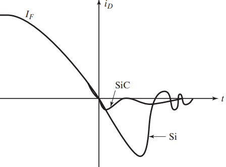
The low reverse recovery characteristic of SiC diodes, as shown in Figure 1, has also a low reverse recovery current.
It saves energy in many applications such as power supplies, solar energy conversion, transportations, and other applications such as welding equipment and air conditioners.
SiC power devices enable increased efficiency, reduced solution size, higher switching frequency, and produce significant less electromagnetic interference (EMI) in a variety of applications.
Silicon Carbide Schottky Diodes
Schottky diodes are used primarily in high frequency and fast-switching applications. Many metals can create a Schottky barrier on either silicon or GaAs semiconductors.
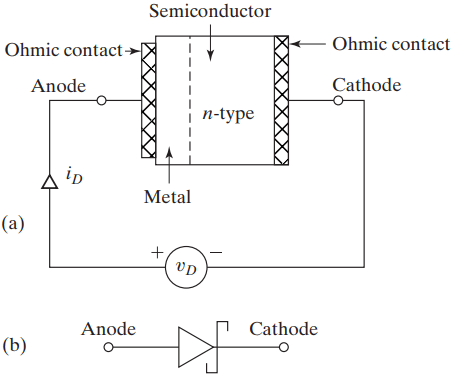
A Schottky diode is formed by joining a doped semiconductor region, usually n-type, with a metal such as gold, silver, or platinum. Unlike a pn-junction diode, there is a metal to semiconductor junction. This is shown in Figure 2a and its symbol in Figure 2b.

The Schottky diode operates only with majority carriers. There are no minority carriers and thus no reverse leakage current as in pn-junction diodes. The metal region is heavily occupied with conduction band electrons, and the n-type semiconductor region is lightly doped.
When forward biased, the higher energy electrons in the n-region are injected into the metal region where they give up their excess energy very rapidly. Since there are no minority carriers, it is a fast-switching diode. The SiC Schottky diodes have the following features:
- Lowest switching losses due to low reverse recovery charge;
- Fully surge-current stable, high reliability, and ruggedness;
- Lower system costs due to reduced cooling requirements;
- Higher frequency designs and increased power density solutions.
These devices also have low device capacitance that enhances overall system efficiency, especially at higher switching frequencies.
Reverse Recovery Characteristics of Power Diodes
The current in a forward-biased junction diode is due to the net effect of majority and minority carriers. Once a diode is in a forward conduction mode and then its forward current is reduced to zero (due to the natural behavior of the diode circuit or application of a reverse voltage), the diode continues to conduct due to minority carriers that remain stored in the pn-junction and the bulk semiconductor material.
The minority carriers require a certain time to recombine with opposite charges and to be neutralized. This time is called the reverse recovery time of the diode.

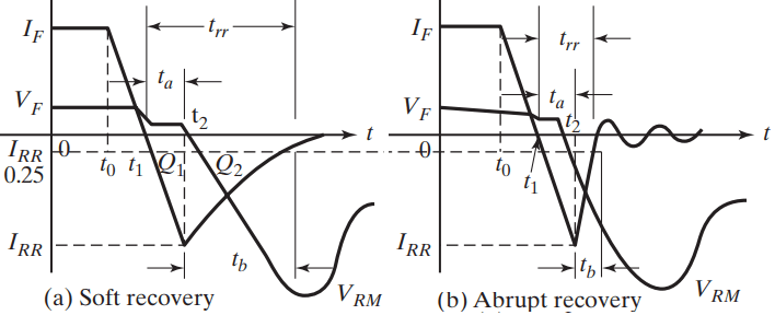
Figure 3 shows two reverse recovery characteristics of junction diodes. It should be noted that the recovery curves in Figure 3 are not scaled and indicate only their shapes. The tailing of the recovery period is expanded to illustrate the nature of recovery although in reality ta > tb.
The recovery process starts at t = t0 when the diode current starts to fall from the on-state current IF at a rate of di/dt = -IF/(t1 – t0). The diode is still conducting with a forward voltage drop of VF.
The forward current IF falls to zero at t = t1 and then continues to flow in the reverse direction because the diode is inactive and not capable of blocking the reverse current flow. At t = t2, the reverse current reaches a value of IRR and the diode voltage starts to reverse.
After the recovery process is completed at t = t3, the reverse diode voltage reaches a peak of VRMS. The diode voltage passes through a transient oscillation period to complete the stored charge recovery until it falls to its normal reverse operating voltage.
The complete process is nonlinear and Figure 3 is used only to illustrate the process.
There are two types of recovery: soft and hard (or abrupt). The soft-recovery type is more common.
The reverse recovery time is denoted as trr and is measured from the initial zero crossing of the diode current to 25% of maximum (or peak) reverse current IRR. The trr consists of two components, ta and tb.
Variable ta is due to charge storage in the depletion region of the junction and represents the time between the zero crossing and the peak reverse current IRR. The tb is due to charge storage in the bulk semiconductor material.
The ratio tb/ta is known as the softness factor (SF). If a diode has SF equals to unity it is known as a soft-recovery diode and for SF less that unity it is known as fast or snappy-recovery diodes.
SF indirectly indicates the voltage transient that occurs upon the turn off of the diode. Low SF implies high transient over-voltage while high SF implies low oscillatory reverse voltage.
For practical purposes, one needs be concerned with the total recovery time trr and the peak value of the reverse current IRR.
trr = ta + tb …….(1)
The peak reverse current can be expressed in reverse di/dt as

Reverse recovery time trr may be defined as the time interval between the instant the current passes through zero during the changeover from forward conduction to reverse blocking condition and the moment the reverse current has decayed to 25% of its peak reverse value IRR.
Variable trr is dependent on the junction temperature, rate of fall of forward current, and forward current prior to commutation, IF.
Reverse recovery charge QRR is the amount of charge carriers that flows across the diode in the reverse direction due to changeover from forward conduction to reverse blocking condition. Its value is determined from the area enclosed by the curve of the reverse recovery current.
That is, QRR = Q1 + Q2.
The storage charge, which is the area enclosed by the curve of the recovery current, is approximately


Equating IRR in Eq. (2) to IRR in Eq. (4) gives

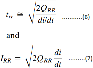
If tb is negligible as compared to ta, which is usually the case (although Figure 3a depicts tb > ta), trr ≈ ta, and Eq. (5) becomes

It can be noticed from Eqs. (6) and (7) that the reverse recovery time trr and the peak reverse recovery current IRR depend on the storage charge QRR and the reverse (or reapplied) di/dt.
The storage charge is dependent on the forward diode current IF. The peak reverse recovery current IRR, reverse charge QRR, and the SF are all of interest to the circuit designer, and these parameters are commonly included in the specification sheets of diodes.
If a diode is in a reverse-biased condition, a leakage current flows due to the minority carriers. Then the application of forward voltage would force the diode to carry current in the forward direction.
However, it requires a certain time known as forward recovery (or turn-on) time before all the majority carriers over the whole junction can contribute to the current flow.
If the rate of rise of the forward current is high and the forward current is concentrated to a small area of the junction, the diode may fail.
Thus, the forward recovery time limits the rate of the rise of the forward current and the switching speed.
Related Posts
- Operation of Thyristors
- Static Characteristics of SCR | Thyristor
- Silicon Controlled Rectifier Function
- Applications & Characteristics of SCR
- SCR Selection Criteria
- Thyristor | SCR Specifications and Ratings
- Operation of Triac & GTO
- Triac Working
- Characteristics, Operation, & Construction of IGBT
- Freewheeling Diode in Controlled Rectifier
- Reverse Recovery Characteristics of Power Diode