J.S. Kilby of Texas Instruments was the first person to develop (in 1959) an integrated circuit — a single monolithic silicon chip in which active and passive components were fabricated by successive deposition, etching and diffusions. He was soon followed by Robert Noyce of Fairchild who successfully fabricated a complete IC including the interconnections on a single silicon chip. Since then the evolution of this technology is fast-paced.
What is an Integrated Circuit?
To put it very briefly, an integrated circuit (IC) is just a packaged electronic circuit. A more detailed definition is as under:-
An IC is a complete electronic circuit in which both the active and passive components are fabricated on a tiny single chip of silicon.
Active components are those which have the ability to produce gain. Examples are – transistors and FETs. Passive components or devices are those which do not have this ability. Examples are – resistors, capacitors and inductors.
ICs are produced by the same processes as are used for manufacturing individual transistors and diodes etc. In such circuits, different components are isolated from each other by isolation diffusion within the crystal chip and are interconnected by an aluminium layer that serves as wires.
A discrete circuit, on the other hand, is one that is built by connecting separate components. In this case, each component is produced separately and then all are assembled together to make the electronic circuit.
Advantages of ICs
As compared to standard printed circuits which use discrete components, ICs have the following advantages:-
1. Extremely small physical size: Often the size is thousands of times smaller than a discrete circuit. The various components and their interconnections are distinguishable only under a powerful microscope
2. Very small weight: Since many circuit functions can be packed into a small space, complex electronic equipment can be employed in many applications where weight and space are critical, such as in aircraft or space-vehicles.
3. Reduced cost: It is a major advantage of ICs. The reduction in cost per unit is due to the fact that many identical circuits can be built simultaneously on a single wafer—this process is called batch fabrication.
Although the processing steps for the wafer are complex and expensive, the large number of resulting integrated circuits make the ultimate cost of each IC fairly low.
4. Extremely high reliability: It is perhaps the most important advantage of an IC and is due to many factors. Most significant factor is the absence of soldered connections. Another is the need for fewer interconnections—the major cause of circuit failures. Small temperature rise due to low power consumptions of ICs also improves their reliability.
In fact, an IC logic gate has been found to be 100,000 times more reliable than a vacuum tube logic gate and 100 times more reliable than a transistor logic gate. Obviously, higher reliability means that ICs will work for longer periods without giving any trouble—something most desirable from both military and consumer application point of view.
5. Increased response time and speed: Since various components of an IC are located close to each other in or on a silicon wafer, the time delay of signals is reduced. Moreover, because of the short distances, the chance of stray electrical pickup (called parasitic capacitance) is practically nil.
Hence it makes them very suitable for small signal operation and high frequency operation. As a result, the response time or the operating speed of the system is improved.
6. Low power consumption: Because of their small size, ICs are more suitable for low power operation than bulky discrete circuits.
7. Easy replacement: ICs are hardly ever repaired because in case of failure, it is more economical to replace them than to repair them.
8. Higher yield: The yield is the percentage of usable devices. Because of the batch fabrication, the yield is very high. Faulty devices usually occur because of some defect in the silicon wafer or in the fabrication steps. Defects in silicon wafer can occur because of lattice imperfection and strains introduced in crystal growth, cutting and handling of the wafers.
Usually such defects are extremely small, but their presence can ruin devices built on or around. Reducing the size of each device greatly increases the chance for a given device to be free of such defects. The same is true for fabrication defects such as the presence of a dust particle on the photolithographic mask.
Drawbacks of ICs
The integrated circuits suffer from the following drawbacks:-
- coils or inductors cannot be fabricated,
- ICs function at fairly low voltages,
- they handle only limited amount of power,
- they are quite delicate and cannot withstand rough handling or excessive heat.
However, the advantages of ICs far outweigh their disadvantages or drawbacks.
Scale of Integration
Level of integration in ICs has been increasing ever since they were developed some three and a half decades back. The number of electronic circuits or components that can be fitted into a standard size IC has been dramatically increasing with each passing year.
In fact, whole electronic systems rather than just a circuit are incorporated in one package. An approximate method of classifying the amount of circuit or component density is as follows:-
1. SSI – small scale integration: In this case, the number of circuits contained in one IC package is less than 12 (or number of components is less than 50).
2. MSI – medium scale integration: Here, number of circuits per package is between 13 and 99 (or number of components is between 50 and 5000).
3. LSI – large scale integration: In this case, circuit density is between 100 and 9,999 (or component density is between 5000 and 100,000).
4. VLSI – very large scale integration: Here the number of circuits per package is between 10,000 to 99,999 (or number of components is between 100,000 – 1,000,000).
5. ULSI – ultra large scale integration: In this case, the circuit density is between 100,000 to 999,999 (or component density is between 1,000,000 – 10,000,000).
6. GSI – Giga scale integration: Here the number of circuits per package is 1,000,000 or more (or number of components are over 100,000,000).
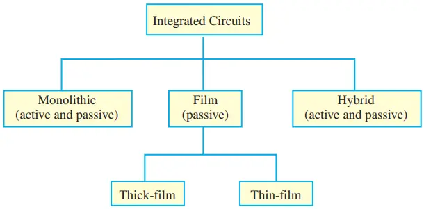
Classification of ICs by Structure
Structurally speaking, ICs can be classified into the following three types:-
1. Monolithic Integrated Circuits: The word ‘monolithic’ means ‘single stone’ or more appropriately ‘a single-solid structure’. In this IC, all circuit components (both active and passive) are fabricated inseparably within a single continuous piece of silicon crystalline material called wafer (or substrate). All components are atomically part of the same chip. Transistors, diodes and other passive components are fabricated at appropriate spots in the substrate using epitaxial diffusion technique.
Component interconnections are provided on the surface of the structure and external connecting wires are taken out to the terminals. It is a complete circuit requiring no ‘add ons’.
Despite some of its distinct disadvantages, monolithic ICs are in wide use because for mass production, monolithic process has been found to be the most economical.
2. Thick and Thin-Film ICs: The essential difference between thick-film and thin-film ICs is not their relative thickness but the method of depositing the film. Both have similar appearance, properties and general characteristics though they both differ in many respects from monolithic ICs.
These ICs are not formed within a silicon wafer but on the surface of an insulating substrate such as glass or a ceramic material. Moreover, only passive components (resistors, capacitors) are formed through thick or thin-film techniques on the insulating surface.
The active elements (transistors, diodes) are added externally as discrete elements to complete a functional circuit. These discrete active components are frequently produced by using the monolithic process.
As stated above, the primary difference between the thick and thin film techniques is the process used for forming passive components and the metallic conduction pattern.
(a) Thin-film ICs: Such circuits are constructed by depositing films (typically 0.1 to 0.5 µm) of conducting material through a mask on the surface of a substrate made of glass or ceramic.
Resistors and conductors are formed by varying the width and thickness of the film and by using materials of different resistivity. Capacitors are produced by sandwiching an insulating oxide film between two conducting films.
Small inductors can be made by depositing a spiral formation of film. The active components like transistors and diodes etc. are externally added and inter-connected by wire bonds. Following two methods are used to produce thin films:-
- vacuum evaporation: In this method, the vaporised material is deposited through a set of masks on the glass or ceramic substrate contained in vacuum.
- cathode sputtering: In this method, atoms from a cathode made of the desired film material are deposited on the substrate which is located between the cathode and the anode.
(b) Thick-film ICs: Such type of integrated circuits are sometimes referred to as printed thin-film circuits. They are so called because silk-screen printing techniques are employed to create the desired circuit pattern on the surface of the substrate.
The screens are made of fine stainless steel wire mesh and the ‘inks’ are pastes (of pulverised glass and aluminium) which have conductive, resistive or dielectric properties. After printing, the circuits are high-temperature fired in a furnace to fuse the films to the insulating substrate. As with thin-film ICs, active elements are added externally as discrete components.
3. Hybrid or Multichip ICs: As the name implies, such circuits are formed either by inter-connecting a number of individual chips or by a combination of film and monolithic IC techniques.
In such ICs, active components are first formed within a silicon wafer (using monolithic technique) which is subsequently covered with an insulating layer such as SiO2.
Film techniques are then employed to form passive components on the SiO2 surface. Connections are made from the film to the monolithic structure through ‘windows’ cut in the SiO2 layer.
Comparison between Different ICs
Each type of IC has its own advantages and disadvantages.
Monolithic circuits have the advantage of lowest cost and highest reliability. However they have the following disadvantages:-
- isolation between components is poorer,
- range of values of passive components used in the circuits is comparatively small,
- inductors cannot be fabricated,
- they afford no flexibility in circuit design because for making any changes in the circuit, a new set of masks is required.
The film circuits have the advantage of forming passive components with broader range of values and reduced tolerances as compared to monolithic circuits. Isolation between their components is also better since they are deposited on a substrate that is an insulator.
Use of external discrete active components allows greater flexibility in circuit design. These circuits also give better high frequency performance than monolithic circuits. However, they suffer from the disadvantages of
- not being able to fabricate active components,
- comparatively higher cost and
- larger physical size.
The chief advantage of multichip ICs is their greater flexibility but they are too expensive for mass production and have least reliability. Hence, such circuits are generally used as prototypes for monolithic ICs. The various integrated circuits are arranged in the form of an ‘IC’ tree of Fig. 1.
Classification of ICs by Function
The earlier classification of ICs was based on their method of construction. However, the integrated circuits can also be classified according to their general function. The two most important categories are:-
- linear and
- digital
Linear Integrated Circuits (LICs)
LICs are also referred to as analog ICs because their inputs and outputs can take on a continuous range of values and the outputs are generally proportional to the inputs. As compared to digital ICs, LICs are used much less.
But LICs are quickly displacing their discrete circuit counterparts in many applications as their cost becomes competitive. They also possess much higher reliability because so many external connections (major source of circuit failure) are eliminated.
LICs find wide use in military and industrial applications as well as in consumer products. They are frequently used in operational amplifiers, small-signal amplifiers, power amplifiers, RF and IF amplifiers, microwave amplifiers, multipliers, voltage comparators, voltage regulators etc. Operational amplifier is by far the most versatile form for an LIC.
Manufacturer’s Designation of LICs: Each manufacturer assigns a specific code and type number to the LICs produced by him.
For example, an internally-compensated op-amp 741 produced by Fairchild is designated as µA 741. Here, µA is the identifying code used by Fairchild. Many other manufacturers produce LICs similar to 741 but use their own code while retaining the same type number.
For example, Fiarchild’s original µA 741 is manufactured by other manufacturers with the following codes:-
- National Semiconductor — LM 741
- Motorola — MC 1741
- RCA — CA 3741
- Texas Instruments — SN 5274
It is seen that the last three digits in each manufacturer’s designation are the same i.e. 741. All these op-amps have the same specifications. Hence, in practice, the manufacturer’s code number is often ignored and all such LICs are referred to as 741.
Many LICs are available in different classes such as A, B, C, E, S and SC. For example, main classes of 741 are as under:-
- 741 —Military grade op-amp
- 741 C — Commercial grade op-amp
- 741 A — Improved version of 741
- 741 E — Improved version of 741 C
- 741 S — Military grade op-amp with higher slew rate
- 741 SE — Commercial grade op-amp with higher slew rate
Digital Integrated Circuits
About 80 per cent of the IC market has been captured by digital ICs which are mostly utilized by the computer industry. Digital ICs lend themselves easily to monolithic integration because a computer uses a large number of identical circuits.
Moreover, such circuits employ relatively few capacitors and values of resistances, voltages and currents are low. Digital ICs contain circuits whose input and output voltages are limited to two possible levels— low or high. It is so because digital signals are usually binary.
Sometimes, digital circuits are referred to as switching circuits. Digital ICs include circuits such as: logic gates, flip-flops, counters, clock-chips, calculator chips, memory chips, microprocessors (µP) etc.
Packaging of ICs
Fig. 2 shows various types of the packaging of ICs used these days. As seen from this figure, the packages can be broadly classified into the following two categories:-
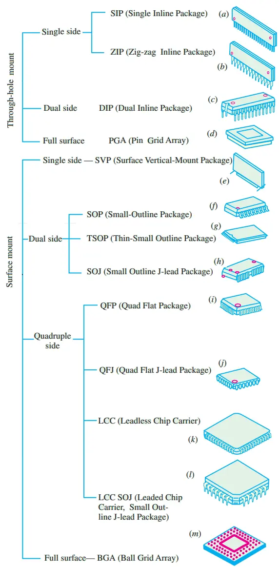
1. through-hole mount that involve inserting the package pins through holes on the printed circuit board (PCB) before soldering [Fig. 2 (a) through (d)].
2. surface mount type where the leads do not pass through holes in the PCB. Instead, surfacemounted package leads are aligned to electrical contacts on the PCB, and are connected simultaneously by solder reflow [Fig. 2 (e) through (m)].
Most packages can be made using ceramic or plastic. The ICs are hermetically sealed for protection from the environment. The pins can be on one side (single inline or zigzag pattern of leads), two sides (dual inline package or DIP), or four sides of the package (quad package).
Most advanced packages have leads distributed over a large portion of the surface of the package as in through-hole pin grid arrays (PGAs) or surface-mounted ball grid arrays (BGAs).