Operational amplifiers (op-amps) are analog circuit components that require power to operate. They are widely used in amplification and signal-conditioning circuits.
The symbol for an op-amp is shown in Figure 1. The symbol is a triangle, with two leads drawn on one side of the triangle, and the third lead is drawn at the apex opposite to that side.
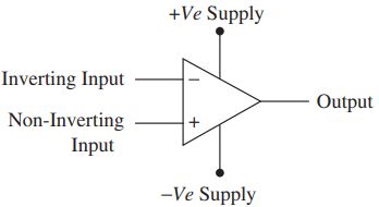
for an op-amp.
One lead is defined as the inverting input (-), the other lead is defined as the non-inverting input (+), and the third lead is the output. The voltages at these two inputs and at the op-amp output are referenced to the ground.
Figure 1 also shows the connections for the positive and negative supply voltages, although these connections are normally omitted when an op-amp is drawn in a circuit. The supply voltage is typically ±15 V.
There are two other connections to the op-amp (called the balance or null offset) that permit adjustment of the op-amp output, but they are typically not shown.
Op Amp | Operational Amplifier Basics
Commercially, op-amps are available in a variety of forms. A common form is the single op-amp in the form of an 8-pin integrated circuit (IC), an example of which is the LM741 chip from National Semiconductor. The pin-layout of this chip is shown in Figure 2(a).
Note that there is no connection to pin 8, and the positive and negative supply voltages are connected at pins 7 and 4, respectively.
Another form is the dual op-amps on a single 8-pin package, and the pin layout for this form is different than that of single op-amp IC. Many vendors manufacture op-amp ICs, and they are available in other chip numbers such as the LF411 chip that is also available from National Semiconductor.
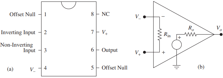
An op-amp is constructed from a number of components including transistors, diodes, capacitors, and resistors.
An ideal op-amp can be modeled as shown in Figure 2(b). The inputs to the op-amp can be thought to be connected internally by a high-impedance resistor Rin. The value of this resistance is high enough (more than 1 M Ω), such that for ideal behavior, we can assume that no current flows between the V– and V+ input terminals.
The output of the op-amp is modeled as a voltage source connected to a low impedance resistor Ro (less than 100 Ω) in series.
The voltage output is proportional to the difference between the input voltages, i.e.,
Vo = KOL x (V+ – V–)
where KOL is the open-loop gain of the op-amp. The open-loop gain of the op-amp is usually very high (105 to 106 ), so a very small voltage difference between the two inputs results in a saturation of the output.
For example, if the gain is 106 , and the saturation voltage is 10 V, then the op-amp will saturate if the voltage difference between the input leads exceeds 10 µV.
Since the op-amp output is finite, but the op-amp has a very large gain, we assume that V+ = V–. The assumption that V+ = V– along with the assumption that no current flows into the input terminals are the two basic rules that are used to analyze ideal op-amp circuits.
It should be noted that the saturation voltage of an op-amp is a function of the supply voltage for the op-amp and it is slightly smaller than it. For example, at supply voltage of ±15 V, the saturation voltage is about ±13 V.
The open-loop input output relationship for an op-amp is shown in Figure 3.
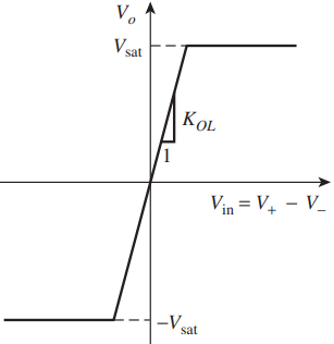
In most cases, however, op-amps are not used in open-loop configuration but are used with a feedback loop between the output voltage lead and the inverting input lead. The closed-loop gain is much smaller than the open-loop gain, but the feedback provides more stable operating characteristics.
Note that an op-amp gives a zero output if the two input voltages are the same. This is called the common-mode rejection property of the op-amp. In reality, the output will not be exactly zero, but one can use the null offset terminals on the op-amp to adjust this output.
Op-amps have good frequency response characteristics, and their bandwidth exceeds 1 MHz. Op-amps can perform various operations such as comparison, amplification, inversion, summation, integration, differentiation, or filtering.
The particular operation depends on how the op-amp is wired and what external components are connected to the op-amp. We will discuss below some of these operations assuming ideal behavior. In most cases, the real-behavior closely follows the ideal behavior.
Comparator OP-AMP
A comparator is used to compare two voltage signals, and switch the output to +Vsat if one of the signals is larger than the other, and to -Vsat otherwise, where Vsat is the saturated output of the op-amp. The circuit for an op-amp operating as a comparator is shown in Figure 2.27.

circuit.
Here the op-amp is operating in open-loop, which means there is no feedback from the op-amp output to the input. The input voltage Vi is connected to the non-inverting input (+), and the reference voltage Vref is connected to the inverting input (-). The comparator output Vo is then

A comparator can be used, as an example, in situations where it is needed to set an output on if a sensor input exceeds a certain value.
Inverting OP-AMP
The inverting op-amp circuit is shown in Figure 4 which has a feedback loop between the op-amp output and the inverting input (-).
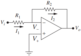
circuit.
An input voltage Vi is applied to the inverting input through a resistor R1, and the non-inverting input (+) is grounded. Since the non-inverting input is connected to ground,
V– = V+ = 0
The current I1 is equal to I2 because virtually no current flows between the inverting and the non-inverting inputs. The current I1 is equal to
I1 = (Vi – V–)/R1 = Vi/R1
and the current I2 is equal to
I2 = (V– – Vo)/R2 = -Vo/R2
Equating I1 to I2, and solving for the op-amp output Vo gives
Vo = -R2Vi/R1
Thus in this circuit the op-amp inverts the input voltage and amplifies it by a factor equal to the ratio of the resistance of R2 to R1.
An application of this circuit is to perform signal inversion where the output will have a 180° phase shift with the input.
Non-inverting OP-AMP
The non-inverting op-amp circuit is shown in Figure 5. Here the non-inverting input (+) is connected to an input voltage Vi, and the inverting input (-) is connected to ground through a resistor R1. There is also a feedback loop between the op-amp output and the inverting input.
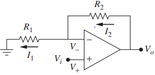
op-amp circuit.
The voltage V+ is equal to V– and is also equal to Vi in this case. But the voltage at the inverting input is also given by

since R1 and R2 act as a voltage-dividing circuit between Vo and ground. Thus, the output Vo of the op-amp is given by

Notice how the gain of the op-amp in this case is always greater than 1.
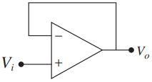
Now if we let R2 to be zero and R1 to be infinite, this gives the circuit shown in Figure 6. This circuit is known as a voltage follower or buffer, and Vo = Vi in this case.
Because the op-amp has a low output impedance (about 75 Ω), and a high input impedance (about 2 M Ω), the voltage follower circuit can be used in a variety of ways to reduce loading effects.
The output of a voltage source can be connected to the buffer input to isolate the source from the rest of the circuit, or the buffer output can be connected to a high-impedance circuit.
Note that in both the inverting and the non-inverting op-amp circuits shown above, the feedback between the output voltage and the inverting input is known as negative feedback. Negative feedback results in a linear relationship between the output and input voltages.
If the feedback loop was between the output voltage and the non-inverting input, then the output-input relationship is nonlinear. The nonlinearity is a hysteresis where the input has to change by a certain amount before the output changes state.
Non-linear op-amp circuits are utilized in the design of Schmitt triggers, which are IC circuits that are used for converting slowly changing or noisy analog signals into two-level digital signals.
The symbol for a standard (non-inverting) Schmitt trigger and the input and output voltages from a Schmitt trigger are shown in Figure 7.

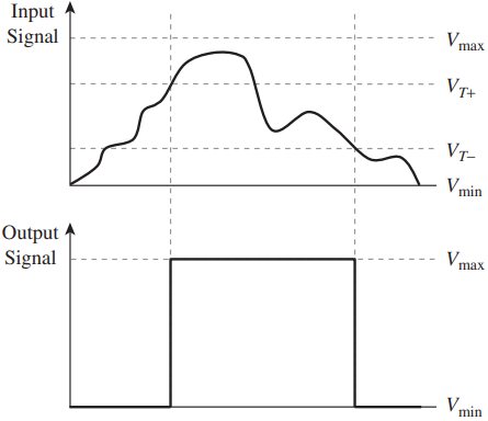
Note how the output of the Schmitt trigger goes to Vmax when the input signal voltage exceeds the positive going threshold voltage (VT+). The output signal stays at Vmax until the input signal drops below the negative going threshold voltage (VT-), at which point the output goes to Vmin.
In Figure 7, Vmax and Vmin are the positive (typically 5 VDC) and the negative (typically 0 VDC) supply voltage, respectively, for the Schmitt trigger device.
The 74HC7014 IC has six non-inverting Schmitt triggers with VT+ = 3.1 V and VT- = 2.9 V when used with a 5 VDC supply voltage.
Differential OP-AMP
An op-amp circuit with two voltages (V1 and V2) applied to its inputs is shown in Figure 8. Two inputs (differential input) are used to reduce the circuit sensitivity to noise, since any noise applied to the circuit will be most probably the same on each of the inputs.
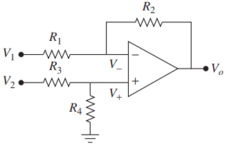
op-amp circuit.
For this circuit, the current through the R1 and the R2 resistors is the same, since no current goes through the inverting input. This current is given by
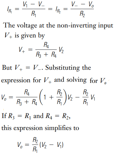
and shows that the output of this op-amp circuit is proportional to the voltage difference between the inputs V2 and V1.
A differential amplifier circuit can be used, for example, to implement an analog proportional control feedback loop (see Figure 9).

feedback loop.
If the reference signal VR is the V2 voltage, the actual or measured signal VA is the V1 voltage, and the ratio R2/R1 is the proportional gain Kp, then the output of the differential amplifier will be
Another application of the differential amplifier circuit is to amplify the difference between the voltage outputs from the arms of a Wheatstone bridge used to measure strain.
Integrating OP-AMP
The circuit for an integrating op-amp is shown in Figure 10, which has a capacitor C in the feedback loop.
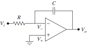
op-amp circuit
The current through a capacitor is given by
IC = Cdv/dt
For this capacitor Vo = V– – Vo = -Vo, since V– = 0. But the current through this capacitor is the same as the current that passes through the resistor R, since no current flows through V–. This current is given by
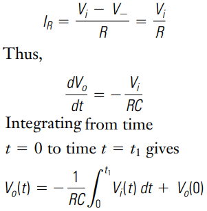
where Vo(0) is the initial condition for the capacitor voltage. Thus, in this circuit, the op-amp produces an inverted output of the integral of the applied input voltage.
Note that if the capacitor and the resistor were interchanged in this circuit, the op-amp will act as a differentiator of the input signal.
The op-amp output in this case will be
Vo = -RC dvi(t)/dt
Note that any noise in the input signal will be amplified by differentiation.
Power Amplifier
A standard op-amp (such as the LM741) has a current output rating of about 25 mA. This is not sufficient to meet the current needs of driving loads (such as valve actuators, servo motors, and audio amplifiers).
Commercial op-amps with a higher current output rating are available. These op-amps are called power op-amps, an example of which is the OPA547 chip from Texas Instruments. The OP547 can provide a continuous output current of 500 mA with the ability to control the output current limit.
Power op-amps can be conveniently used to interface a digital-to-analog (D/A) converter that needs to drive a DC motor. Table 1 gives a sampling of power op-amp devices.
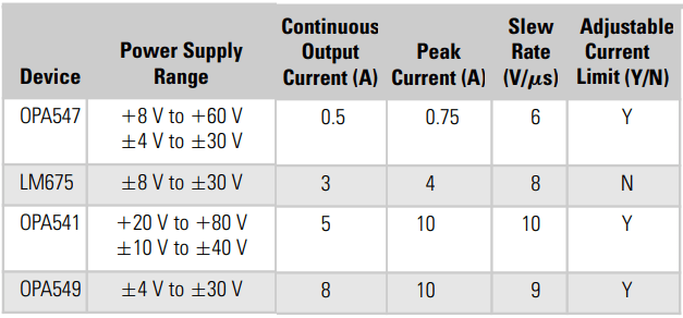
In Table 1, the ‘Power Supply Range’ column defines the allowable voltage levels that can be applied to the positive and negative supply inputs of the op-amp. The power supply range affects the op-amp output voltage swing, which is the maximum voltage that the op-amp can produce without saturation for a given load. Note that the output voltage swing is proportional to the power supply range.
The ‘Slew Rate’ column defines the rate at which the op-amp output voltage will change when the op-amp gain is set to unity. Several of the power op-amps listed in the Table 1 allow adjustment of the maximum output current of the op-amp.
Due to their large output current, power op-amps are available in packages with a built-in copper tab to allow easy mounting to a heat sink for good thermal performance.
Related Posts
- P N Junction Diode Theory | Working
- Characteristics of PN Junction Diode
- Working Principle of Rectifier
- Zener Diode Characteristics
- Zener Diode as Voltage Regulator
- JFET | Junction Field Effect Transistor Basics
- JFET Construction and Working
- Op Amp | Operational Amplifier Basics
- Transistor as a Switch
- Buck Converter Working
- Buck Boost Converter Working
- Astable & Monostable Operation of 555 Timer Chip
- Light Sensitive Devices
- Industrial Applications of Ultrasonic Waves
- Radar Working Principle
- Electrical Timer & Timer Charts
- RLC Parallel & RLC Series Circuit Resonance
- Types of Capacitors