Characteristics of PN junction diode is a graph between the voltage applied across its terminals and the current that flows through it. It is drawn to know the behavior of diode in the electrical circuit.
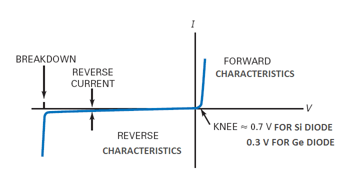
For a typical junction diode, characteristics are shown in Figure. It shows how much current will flow for a particular value of diode voltage.

Forward Characteristics of PN Junction Diode
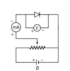
To obtain the forward bias characteristics of PN junction diode, set up the circuit shown in Figure.
In the circuit, a DC battery is connected to the diode through a potentiometer.
The potentiometer helps in varying the voltage applied to the diode. The milli-ammeter measures the current in the circuit. The voltmeter measures the voltage across the diode.

Here, the voltage is plotted along the x-axis, as the voltage is the independent variable. Each value of diode voltage produces a particular current. The current, being the dependent variable, is plotted along the y-axis.
From the curve, we know that the diode current is very small for the first few tenths of a volt. The diode does not conduct well until the external voltage overcomes the barrier potential.
As we approach 0.3 V, a larger number of free electrons and holes start crossing the junction. Above 0.3 V even a small increase in the voltage produces a sharp increase in the current.
A forward voltage, at which the current through the junction starts to increase rapidly, is known as knee voltage (Vo) of the diode.
For a germanium diode, it is approximately 0.3 V, whereas for a silicon diode it is about 0.7 V.
If too large current flows through the diode, excessive heat will destroy it. The maximum current that a diode can handle safely is specified by the manufacturer.
Reverse-Bias Characteristics of PN Junction Diode
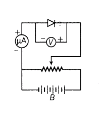
To obtain the reverse-bias characteristics of PN junction diode make the following changes:
- reverse the terminals of battery and note that high voltage battery is used here ,
- replace the milli-ammeter with a micro-ammeter.

In the reverse bias, the diode current is very small. It is only a few µA for germanium diodes and a few nA for silicon diodes.
It remains small and almost constant for all voltages less than the breakdown voltage (Vz). At breakdown voltage, current increases rapidly for a small increase in voltage.
A reverse voltage, at which PN junction breaks down with a sudden rise in reverse current is known as the breakdown voltage of the diode.
The high reverse current may damage the junction. Therefore, for proper operation of a junction diode, reverse voltage across a PN junction should always be less than the breakdown voltage.
Limiting Values of Junction Diode
Every PN junction diode has three limiting values;
- Maximum Forward Current: It is the highest instantaneous forward current that a junction diode can conduct safely.
- Peak Inverse Voltage (PIV): It is the maximum reverse voltage that can be applied to a junction diode without damage to the junction. If the reverse voltage across the diode exceeds its PIV, the diode may be destroyed due to excessive heat.
The peak inverse voltage is very significant when we are using diodes in rectifier circuit. In such applications, reverse voltage across diode during negative half-cycle of AC should not exceed the PIV of a diode.
- Maximum Power Rating: It is the maximum power that can be handled by a diode safely. It is equal to the product of junction current and voltage across the junction.
For safe operation of a diode, these values should not be exceeded. If these are exceeded, a diode may be destroyed due to excessive heat. These are specified by the manufacturer in the data sheets.
Related Posts
- P N Junction Diode Theory | Working
- Characteristics of PN Junction Diode
- Working Principle of Rectifier
- Zener Diode Characteristics
- Zener Diode as Voltage Regulator
- JFET | Junction Field Effect Transistor Basics
- JFET Construction and Working
- Op Amp | Operational Amplifier Basics
- Transistor as a Switch
- Buck Converter Working
- Buck Boost Converter Working
- Astable & Monostable Operation of 555 Timer Chip
- Light Sensitive Devices
- Industrial Applications of Ultrasonic Waves
- Radar Working Principle
- Electrical Timer & Timer Charts
- RLC Parallel & RLC Series Circuit Resonance
- Types of Capacitors
© https://www.yourelectricalguide.com/ forward and reverse bias characteristics of pn junction diode.